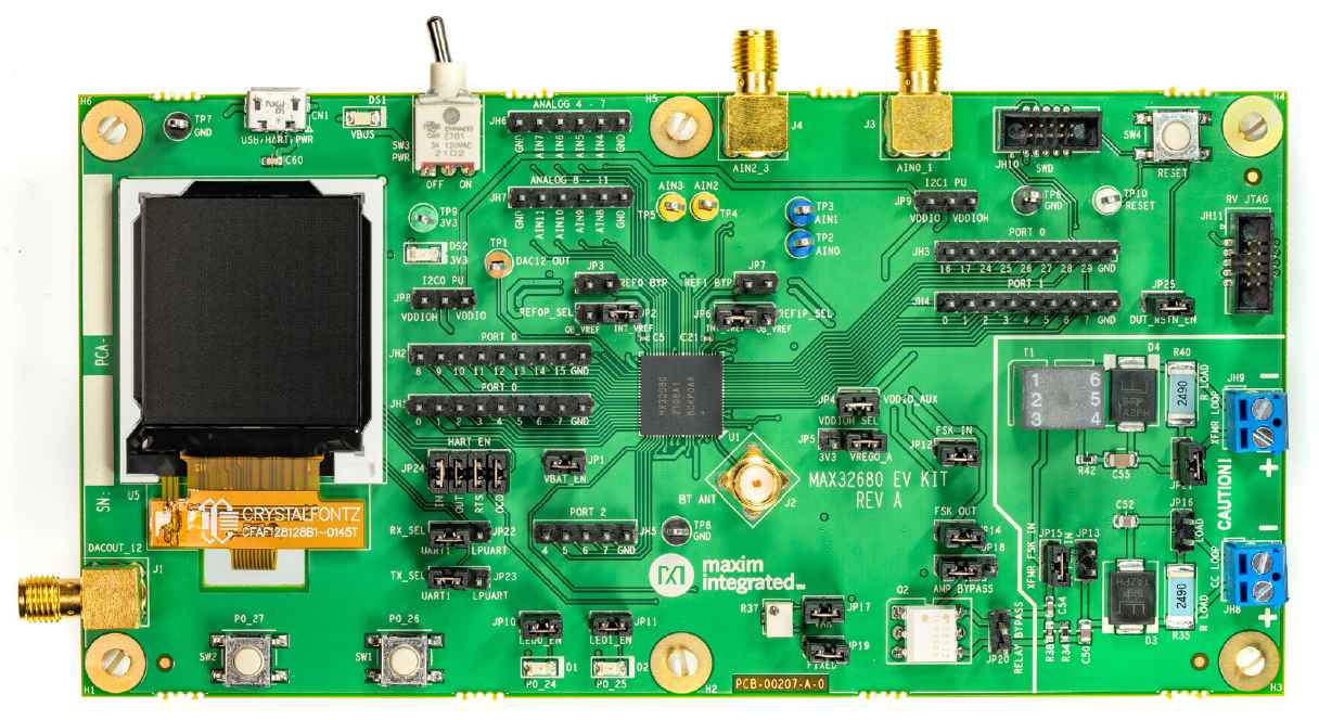
MAX32680EVKIT
Overview
The MAX32680 evaluation kit (EV kit) provides a platform for evaluation capabilities of the MAX32680 microcontroller, which is an advanced system-on-chip (SoC) designed for industrial and medical sensors. Power regulation and management is provided by a single-inductor multiple-output (SIMO) buck regulator system and contains the latest generation Bluetooth® 5.2 Low Energy (LE) radio.
The Zephyr port is running on the MAX32680 MCU.

Hardware
MAX32680 MCU:
Ultra-Low-Power Wireless Microcontroller
Internal 100MHz Oscillator
512KB Flash and 128KB SRAM, Optional ECC on One 32KB SRAM Bank
Bluetooth 5.2 LE Radio
Dedicated, Ultra-Low-Power, 32-Bit RISC-VCoprocessor to Offload
Timing-Critical Bluetooth Processing
Fully Open-Source Bluetooth 5.2 Stack Available
Supports AoA, AoD, LE Audio, and Mesh
High-Throughput (2Mbps) Mode•Long-Range (125kbps and 500kbps) Modes
Rx Sensitivity: -97.5dBm; Tx Power: +4.5dBm
Single-Ended Antenna Connection (50Ω)
Smart Integration Reduces BOM, Cost, and PCB Size
Two 16-Bit to 24-Bit Sigma-Delta ADCs
12 Channels, Assignable to Either ADC
Flexible Resolution and Sample Rates
24-Bits at 0.4ksps, 16-Bits at 4ksps
Four External Input, 10-Bit Sigma-Delta ADC 7.8ksps
12-Bit DAC
On-Die Temperature Sensor
Digital Peripherals: Two SPI, Two I2C, up to FourUART, and up to 36 GPIOs
Timers: Six 32-Bit Timers, Two Watchdog Timers,Two Pulse Trains, 1-Wire® Master
Power Management Maximizes Battery Life
2.0V to 3.6V Supply Voltage Range
Integrated SIMO Power Regulator
Dynamic Voltage Scaling (DVS)
23.8μA/MHz ACTIVE Mode Current at 3.0VCoremark®
4.4μA at 3.0V Retention Current for 32KB SRAM
Selectable SRAM Retention in Low-Power Modes
Robust Security and Reliability
TRNG
Secure Nonvolatile Key Storage and AES-128/192/256
Secure Boot to Protect IP/Firmware
Wide, -40°C to +85°C Operating Temperature
External devices connected to the MAX32680 EVKIT:
SMA Connector for Attaching an External Bluetooth Antenna
128 x 128 (1.45in) Color TFT Display with SPI Interface
Two Selectable On-Board, High-Precision Voltage References
USB 2.0 Micro B to Serial UARTs
UART1 and LPUART0 Interface is Selectable Through On-Board Jumpers
All GPIOs Signals Accessed Through 0.1in Headers
Access to Four Analog Inputs Through SMA Connectors Configured as Differential
Access to Eight Analog Inputs Through 0.1in Headers Configured as Single-End
Optional Discrete Filter for the Twelve Analog Inputs
DAC Accessed Through SMA Connector or Test Point
10-Pin SWD Connector
10-Pin RV JTAG Connector
Board Power Provided by USB Port
On-Board 3.3V LDO Regulator to Power MAX32680 Internal SIMO
Test Loops Provided to Supply Optional VCORE Power Externally
Individual Power Measurement on All IC Rails Through Jumpers
Two General Purpose LEDs and Two General Purpose Pushbutton Switches
Supported Features
Below interfaces are supported by Zephyr on MAX32680EVKIT.
Interface |
Controller |
Driver/Component |
|---|---|---|
NVIC |
on-chip |
nested vector interrupt controller |
SYSTICK |
on-chip |
systick |
CLOCK |
on-chip |
clock and reset control |
GPIO |
on-chip |
gpio |
UART |
on-chip |
serial |
Connections and IOs
Name |
Name |
Settings |
Description |
||||||||||||||||||||||||
|---|---|---|---|---|---|---|---|---|---|---|---|---|---|---|---|---|---|---|---|---|---|---|---|---|---|---|---|
JP1 |
VREGI |
|
|
||||||||||||||||||||||||
JP2 |
REF0P |
|
|
||||||||||||||||||||||||
JP3 |
REF0N |
|
|
||||||||||||||||||||||||
JP4 |
VDDIO_AUX |
|
|
||||||||||||||||||||||||
JP5 |
VDDIOH |
|
|
||||||||||||||||||||||||
JP6 |
REF1P |
|
|
||||||||||||||||||||||||
JP7 |
REF1N |
|
|
||||||||||||||||||||||||
JP8 |
I2C0_SDA I2C0_SCL |
|
|
||||||||||||||||||||||||
JP9 |
I2C1_SDA I2C1_SCL |
|
|
||||||||||||||||||||||||
JP10 |
P0_24 |
|
|
||||||||||||||||||||||||
JP11 |
P0_25 |
|
|
||||||||||||||||||||||||
JP12 |
FSK_IN |
|
|
||||||||||||||||||||||||
JP13 |
RCV_FSK |
|
|
||||||||||||||||||||||||
JP14 |
FSK_OUT |
|
|
||||||||||||||||||||||||
JP15 |
RCV_FSK |
|
|
||||||||||||||||||||||||
JP16 |
RLOAD |
|
|
||||||||||||||||||||||||
JP17 |
FSK AMP GAIN |
|
|
||||||||||||||||||||||||
JP18 |
AMP BYPASS |
|
|
||||||||||||||||||||||||
JP19 |
FSK AMP GAIN |
|
|
||||||||||||||||||||||||
JP20 |
HART_RTS |
|
|
||||||||||||||||||||||||
JP21 |
RLOAD |
|
|
||||||||||||||||||||||||
JP22 |
UART0_RX |
|
|
||||||||||||||||||||||||
JP23 |
UART0_TX |
|
|
||||||||||||||||||||||||
JP24 |
|
|
|
||||||||||||||||||||||||
JP25 |
RSTN |
|
|
Programming and Debugging
Flashing
The MAX32680 MCU can be flashed by connecting an external debug probe to the SWD port. SWD debug can be accessed through the Cortex 10-pin connector, JH10. Logic levels are set to 1.8V (VDDIO_AUX).
Once the debug probe is connected to your host computer, then you can simply run the
west flash command to write a firmware image into flash.
Debugging
Please refer to the Flashing section and run the west debug command
instead of west flash.