RA6E1 Fast Prototyping Board
Overview
The Renesas RA6E1 group uses the high-performance Arm® Cortex®-M33 core with TrustZone®. The RA6E1 is suitable for entry IoT applications requiring streamlined feature and connectivity integration including Ethernet, and unprecedented performance with 790.75 CoreMark, which are 3.95CoreMark / Mhz.
The key features of the FPB-RA6E1 board are categorized in three groups as follow:
MCU Native Pin Access
200MHz Arm Cortex-M33 based RA6E1 MCU in 100 pins, LQFP package
Native pin access through 2 x 50-pin male headers (not fitted)
MCU current measurement point for precision current consumption measurement
Multiple clock sources - Low-precision (~1%) clocks are available internal to the RA MCU. RA MCU oscillator and sub-clock oscillator crystals, providing precision 24.000 MHz (not fitted) and 32,768 Hz reference clocks are also available
System Control and Ecosystem Access
Two 5V input sources
USB (Debug, Full Speed, High Speed)
External power supply (using 2-pin header) (not fitted)
Built-in SEGGER J-Link Emulator On-Board programmer/debugger (SWD)
User LEDs and buttons
Two User LEDs (green)
Power LED (green) (not fitted) indicating availability of regulated power
Debug/power LED (yellow) indicating power and the debug connection
One User button
One Reset button
Two popular ecosystems expansions
Two Digilent PmodTM (SPI, UART) connectors (not fitted)
Arduino (Uno R3) connector
MCU boot configuration jumper

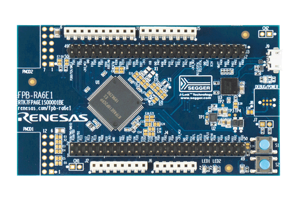
FPB-RA6E1 Board Functional Area Definitions (Credit: Renesas Electronics Corporation)
Hardware
Detailed hardware feature for the RA6E1 MCU group can be found at RA6E1 Group User’s Manual Hardware

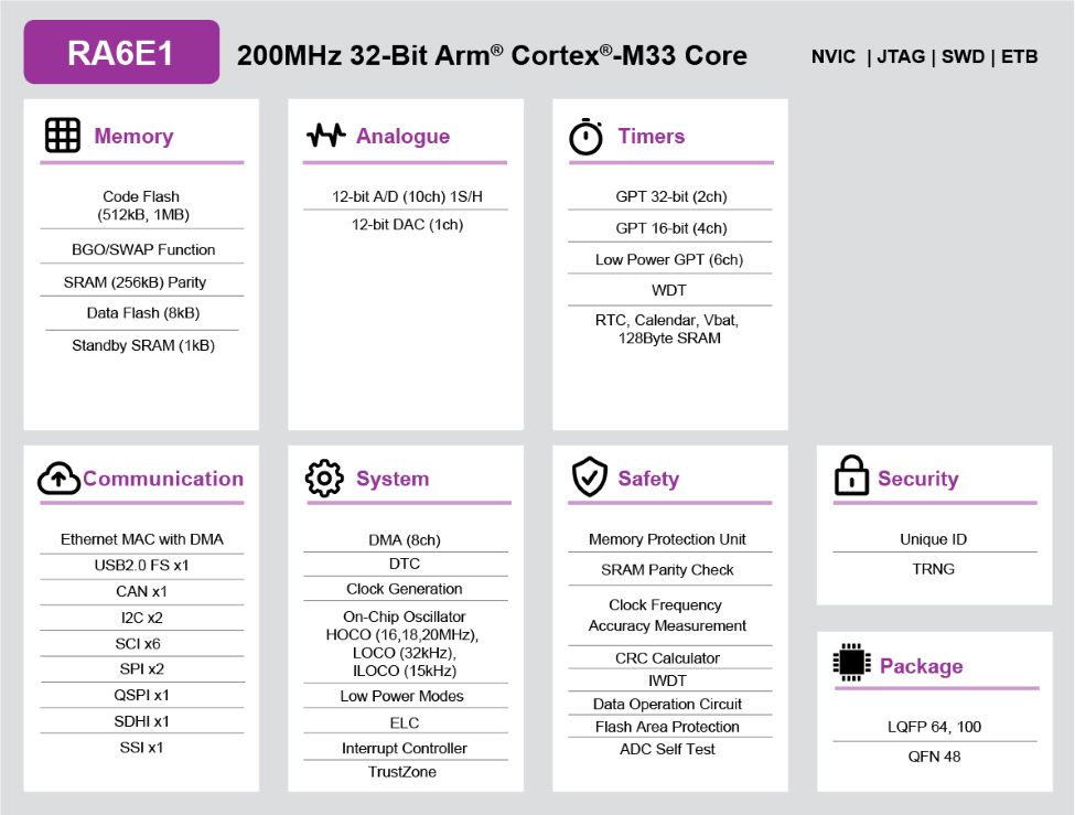
RA6E1 Block diagram (Credit: Renesas Electronics Corporation)
Detailed hardware feature for the FPB-RA6E1 MCU can be found at FPB-RA6E1 - User’s Manual
Supported Features
The below features are currently supported on Zephyr OS for FPB-RA6E1 board:
Interface |
Controller |
Driver/Component |
|---|---|---|
GPIO |
on-chip |
gpio |
MPU |
on-chip |
arch/arm |
NVIC |
on-chip |
arch/arm |
UART |
on-chip |
serial |
FLASH |
on-chip |
flash |
Other hardware features are currently not supported by the port.
Programming and Debugging
Applications for the fpb_ra6e1 board target configuration can be
built, flashed, and debugged in the usual way. See
Building an Application and Run an Application for more details on
building and running.
Flashing
Program can be flashed to FPB-RA6E1 via the on-board SEGGER J-Link debugger. SEGGER J-link’s drivers are avaialbe at https://www.segger.com/downloads/jlink/
To flash the program to board
Connect to J-Link OB via USB port to host PC
Make sure J-Link OB jumper is in default configuration as describe in FPB-RA6E1 - User’s Manual
Execute west command
west flash -r jlink
Debugging
You can use Segger Ozone (Segger Ozone Download) for a visual debug interface
Once downloaded and installed, open Segger Ozone and configure the debug project like so:
Target Device: R7FA6E10F
Target Interface: SWD
Target Interface Speed: 4 MHz
Host Interface: USB
Program File: <path/to/your/build/zephyr.elf>
Note: It’s verified that we can debug OK on Segger Ozone v3.30d so please use this or later version of Segger Ozone