MAX32655EVKIT
Overview
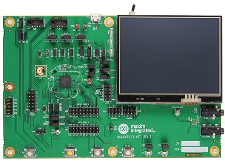
The MAX32655 evaluation kit (EV kit) provides a platform for evaluation capabilities of the MAX32655 microcontroller, which is an advanced system-on-chip (SoC). It features an Arm® Cortex®-M4F CPU for efficient computation of complex functions and algorithms, integrated power management (SIMO), and the newest generation Bluetooth® 5.0 Low Energy (Bluetooth LE), long-range radio for wearable and hearable device applications.
The Zephyr port is running on the MAX32655 MCU.
Hardware
MAX32655 MCU:
- Ultra-Low-Power Wireless Microcontroller
Internal 100MHz Oscillator
Flexible Low-Power Modes with 7.3728MHz System Clock Option
512KB Flash and 128KB SRAM (Optional ECC on One 32KB SRAM Bank)
16KB Instruction Cache
- Bluetooth 5.2 LE Radio
Dedicated, Ultra-Low-Power, 32-Bit RISC-V Coprocessor to Offload Timing-Critical Bluetooth Processing
Fully Open-Source Bluetooth 5.2 Stack Available
Supports AoA, AoD, LE Audio, and Mesh
High-Throughput (2Mbps) Mode
Long-Range (125kbps and 500kbps) Modes
Rx Sensitivity: -97.5dBm; Tx Power: +4.5dBm
Single-Ended Antenna Connection (50Ω)
- Power Management Maximizes Battery Life
2.0V to 3.6V Supply Voltage Range
Integrated SIMO Power Regulator
Dynamic Voltage Scaling (DVS)
23.8μA/MHz Active Current at 3.0V
4.4μA at 3.0V Retention Current for 32KB
Selectable SRAM Retention + RTC in Low-Power Modes
- Multiple Peripherals for System Control
Up to Two High-Speed SPI Master/Slave
Up to Three High-Speed I2C Master/Slave (3.4Mbps)
Up to Four UART, One I2S Master/Slave
Up to 8-Input, 10-Bit Sigma-Delta ADC 7.8ksps
Up to Four Micro-Power Comparators
Timers: Up to Two Four 32-Bit, Two LP, TwoWatchdog Timers
1-Wire® Master
Up to Four Pulse Train (PWM) Engines
RTC with Wake-Up Timer
Up to 52 GPIOs
- Security and Integrity
Available Secure Boot
TRNG Seed Generator
AES 128/192/256 Hardware Acceleration Engine
External devices connected to the MAX32655 EVKIT:
Color TFT Display
Audio Stereo Codec Interface
Digital Microphone
A 128Mb QSPI flash
Supported Features
The max32655evkit board supports the hardware features listed below.
- on-chip / on-board
- Feature integrated in the SoC / present on the board.
- 2 / 2
-
Number of instances that are enabled / disabled.
Click on the label to see the first instance of this feature in the board/SoC DTS files. -
vnd,foo -
Compatible string for the Devicetree binding matching the feature.
Click on the link to view the binding documentation.
max32655evkit/max32655/m4 target
On-target memory for this board target: 64 KiB of RAM, 512 KiB of Flash.
Type |
Location |
Description |
Compatible |
|---|---|---|---|
CPU |
on-chip |
ARM Cortex-M4F CPU1 |
|
on-chip |
MAX32 RV32 core1 |
||
ADC |
on-chip |
ADI MAX32 ADC 10-Bits1 |
|
Clock control |
on-chip |
||
on-chip |
MAX32 Global Control1 |
||
Counter |
on-chip |
ADI MAX32 counter6 |
|
on-chip |
ADI MAX32 compatible Counter RTC1 |
||
on-chip |
ADI MAX32 Wake-Up Timer is a unique instance of a 32-bit timer that can wake up the device from sleep, standby and backup modes1 |
||
DMA |
on-chip |
ADI MAX32 DMA1 |
|
Flash controller |
on-chip |
MAX32XXX flash controller1 |
|
GPIO & Headers |
on-chip |
MAX32 GPIO4 |
|
I2C |
on-chip |
||
I2S |
on-chip |
Analog Devices MAX32 series I2S controller1 |
|
Input |
on-board |
Group of GPIO-bound input keys1 |
|
Interrupt controller |
on-chip |
ARMv7-M NVIC (Nested Vectored Interrupt Controller)1 |
|
LED |
on-board |
Group of GPIO-controlled LEDs1 |
|
Mailbox |
on-chip |
ADI MAX32 SEMA Mailbox1 |
|
MTD |
on-chip |
Flash node1 |
|
on-board |
Properties supporting Zephyr spi-nor flash driver (over the Zephyr SPI API) control of serial flash memories using the standard M25P80-based command set1 |
||
Pin control |
on-chip |
MAX32 Pin Controller1 |
|
PWM |
on-chip |
ADI MAX32 PWM4 |
|
RNG |
on-chip |
ADI MAX32XXX TRNG1 |
|
Serial controller |
on-chip |
||
SPI |
on-chip |
||
SRAM |
on-chip |
Generic on-chip SRAM4 |
|
Timer |
on-chip |
ADI MAX32 timer7 |
|
on-chip |
ARMv7-M System Tick1 |
||
1-Wire |
on-chip |
ADI MAX32xxx MCUs 1-Wire Master1 |
|
Watchdog |
on-chip |
max32655evkit/max32655/rv32 target
On-target memory for this board target: 64 KiB of RAM, 512 KiB of Flash.
Type |
Location |
Description |
Compatible |
|---|---|---|---|
CPU |
on-chip |
MAX32 RV32 core1 |
|
ADC |
on-chip |
ADI MAX32 ADC 10-Bits1 |
|
Clock control |
on-chip |
||
on-chip |
MAX32 Global Control1 |
||
Counter |
on-chip |
ADI MAX32 counter6 |
|
on-chip |
ADI MAX32 compatible Counter RTC1 |
||
on-chip |
ADI MAX32 Wake-Up Timer is a unique instance of a 32-bit timer that can wake up the device from sleep, standby and backup modes1 |
||
DMA |
on-chip |
ADI MAX32 DMA1 |
|
Flash controller |
on-chip |
MAX32XXX flash controller1 |
|
GPIO & Headers |
on-chip |
MAX32 GPIO4 |
|
I2C |
on-chip |
ADI MAX32 I2C3 |
|
I2S |
on-chip |
Analog Devices MAX32 series I2S controller1 |
|
Input |
on-board |
Group of GPIO-bound input keys1 |
|
Interrupt controller |
on-chip |
MAX32 RV32 Core Interrupt Controller1 |
|
LED |
on-board |
Group of GPIO-controlled LEDs1 |
|
Mailbox |
on-chip |
ADI MAX32 SEMA Mailbox1 |
|
MTD |
on-chip |
Flash node1 |
|
Pin control |
on-chip |
MAX32 Pin Controller1 |
|
PWM |
on-chip |
ADI MAX32 PWM4 |
|
RNG |
on-chip |
ADI MAX32XXX TRNG1 |
|
Serial controller |
on-chip |
||
SPI |
on-chip |
ADI MAX32 SPI1 |
|
SRAM |
on-chip |
Generic on-chip SRAM4 |
|
Timer |
on-chip |
ADI MAX32 timer6 |
|
on-chip |
ADI MAX32 RV32 system timer1 |
||
1-Wire |
on-chip |
ADI MAX32xxx MCUs 1-Wire Master1 |
|
Watchdog |
on-chip |
MAX32XXX watchdog2 |
Connections and IOs
Name |
Signal |
Usage |
|---|---|---|
JP1 |
VREGI |
Connect/Disconnect VREGIO power |
JP2 |
P0_24 |
Enable/Disable LED1 |
JP3 |
P0_25 |
Enable/Disable LED2 |
JP4 |
P2_6/ P2_7 |
Connect/Disconnect the USB to serial UART to GPIO P2_6 (LPUART_RX) |
JP5 |
P2_7/ P0_1 |
Connect/Disconnect the USB to serial UART to GPIO P2_7 (LPUART_TX) |
JP6 |
P0_2 |
Connect/Disconnect the USB to serial UART to GPIO P0_2 (UART0_CTS) |
JP7 |
P0_3 |
Connect/Disconnect he USB to serial UART to GPIO P0_3 (UART0_RTS) |
JP8 |
VREGI |
Select VDDIO_EN power source (3V3 or coin cell) |
JP9 |
VDDIOH_EN |
Select VDDIOH_EN power source 3V3/VREGI |
JP10 |
VDDIOH |
Connect/Disconnect VDDIOH power |
JP11 |
VDDIO_EN |
Select VDDIO_EN power source 1V8/VREGO_A |
JP12 |
VDDIO |
Connect/Disconnect VDDIO power |
JP13 |
VDDA_EN |
Select VDDA_EN power source 1V8/VREGO_A |
JP14 |
VDDA |
Connect/Disconnect VDDA power |
JP15 |
VCOREA_EN |
Select VCOREA_EN power source 1V1/VREGO_C |
JP16 |
VCOREA |
Connect/Disconnect VCOREA power |
JP17 |
VCOREB_EN |
Select VCOREB_EN power source 1V1/VREGO_B |
JP18 |
VCOREB |
Connect/Disconnect VCOREB power |
JP19 |
BLE_LDO |
Connect/Disconnect BLE_LDO power |
JP20 |
VREF |
Select VREF power source VDDIO/VDDIOH |
JP21 |
I2C0_PU |
Select I2C0_PU power source VDDIO/VDDIOH |
JP22 |
I2C1_PU |
Select I2C1_PU power source VDDIO/VDDIOH |
JP23 |
BOARD RESET |
Connect/Disconnect RV JTAG NRESET from the BOARD RESET circuitry |
Programming and Debugging
The max32655evkit board supports the runners and associated west commands listed below.
| flash | debug | debugserver | attach | rtt | reset | |
|---|---|---|---|---|---|---|
| jlink | ✅ | ✅ | ✅ | ✅ | ✅ | ✅ |
| openocd | ✅ (default) | ✅ (default) | ✅ | ✅ | ✅ |
Flashing
The MAX32655 MCU can be flashed by connecting an external debug probe to the SWD port. SWD debug can be accessed through the Cortex 10-pin connector, JH3. Logic levels are fixed to VDDIO (1.8V).
Once the debug probe is connected to your host computer, then you can simply run the
west flash command to write a firmware image into flash. To perform a full erase,
pass the --erase option when executing west flash.
Note
This board uses OpenOCD as the default debug interface. You can also use
a Segger J-Link with Segger’s native tooling by overriding the runner,
appending --runner jlink to your west command(s). The J-Link should
be connected to the standard 2*5 pin debug connector (JW3) using an
appropriate adapter board and cable.
Debugging
Please refer to the Flashing section and run the west debug command
instead of west flash.
Dual Core Support
An experimental board ID for the secondary RISC-V core is available with ID
max32655evkit/max32655/m4.
The primary Arm core uses Kconfig options,
CONFIG_MAX32_SECONDARY_RV32 to enable the secondary
RISC-V core. The devicetree chosen property zephyr,code-rv32-partition,
is used to determine the address for the RV32 core to start executing.
Hello World for multiple board targets using Sysbuild supports building the Arm and RISC-V images:
west build -b max32655evkit/max32655/m4 -T sample.sysbuild.hello_world samples/sysbuild/hello_world
Currently, flashing both images requires using the JLink runner with a connected JLink device:
west build -b max32655evkit/max32655/m4 samples/sysbuild/hello_world
west flash -r jlink
To view the console for the RV32 core using the USB connection on the kit, move jumpers JP4 and JP5 to their “LP” positions.