MAX32666FTHR
Overview
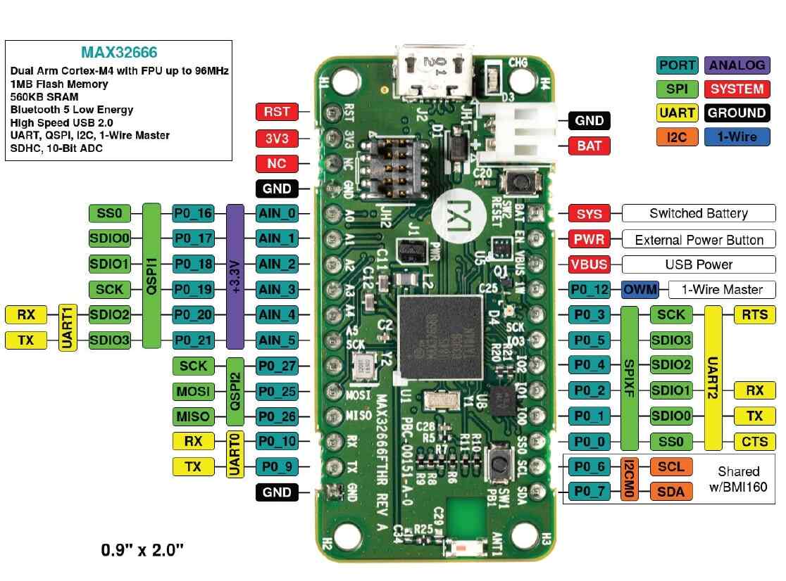
The MAX32666FTHR board is a rapid development platform to help engineers quickly implement battery optimized Bluetooth® 5 solutions with the MAX32666 Arm® Cortex®-M4 processor with FPU. The board also includes the MAX1555 1-Cell Li+ battery charger for battery management. The form factor is a small 0.9in by 2.0in dualrow header footprint that is compatible with breadboards and off-the-shelf peripheral expansion boards. The board also includes a variety of peripherals, such as a micro SD card connector, 6-axis accelerometer/gyro, RGB indicator LED, and pushbutton. This platform provides poweroptimized flexible for quick proof-of-concepts and early software development to enhance time to market.
The Zephyr port is running on the MAX32666 MCU.
Hardware
MAX32666 MCU:
High-Efficiency Microcontroller and Audio DSP for Wearable and Hearable Devices
Arm Cortex-M4 with FPU Up to 96MHz
Optional Second Arm Cortex-M4 with FPU Optimized for Data Processing
Low-Power 7.3728MHz System Clock Option
1MB Flash, Organized into Dual Banks 2 x 512KB
560KB (448KB ECC) SRAM; 3 x 16KB Cache
Optional Error Correction Code (ECC-SEC-DED)for Cache, SRAM, and Internal Flash
Bluetooth 5 Low Energy Radio
1Mbps and 2Mbps Data Throughput
Long Range (125kbps and 500kbps)
Advertising Extension
Rx Sensitivity: -95dbm; Tx Power Up to +4.5dbm
On-Chip Matching with Single-Ended Antenna Port
Power Management Maximizes Operating Time for Battery Applications
Integrated SIMO SMPS for Coin-Cell Operation
Dynamic Voltage Scaling Minimizes Active Core Power Consumption
27.3μA/MHz at 3.3V Executing from Cache
Selectable SRAM Retention in Low Power Modes with RTC Enabled
Multiple Peripherals for System Control
Three QSPI Master/Slave with Three Chip Selects Each
Three 4-Wire UARTs
Three I2C Master/Slave
Up to 50 GPIO
QSPI (SPIXF) with Real-Time Flash Decryption
QSPI (SPIXR) RAM Interface Provides SRAMExpansion
8-Input 10-Bit Delta-Sigma ADC 7.8ksps
USB 2.0 HS Engine with Internal Transceiver
PDM Interface Supports Two Digital Microphones
I2S with TDM
Six 32-Bit Timers
Two High-Speed Timers
1-Wire Master
Sixteen Pulse Trains (PWM)
Secure Digital Interface Supports SD3.0/SDIO3.0/eMMC4.51
Secure Valuable IP/Data with Hardware Security
Trust Protection Unit (TPU) with MAA SupportsFast ECDSA and Modular Arithmetic
AES128/192/256, DES, 3DES, Hardware Accelerator
TRNG Seed Generator
SHA-2 Accelerator•Secure Bootloader
External devices connected to the MAX32666FTHR:
MAX1555 1-Cell Li+ Battery Charger
Breadboard Compatible Headers
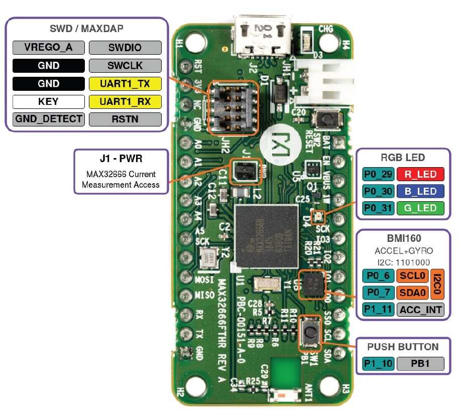
10-Pin Cortex Debug Header
Micro USB Connector
Micro SD Card Connector
RGB Indicator LED and One General Purpose Push Button Switch
6-Axis Accelerometer/Gyro
Bluetooth Surface Mount Antenna
Supported Features
The max32666fthr board supports the hardware features listed below.
- on-chip / on-board
- Feature integrated in the SoC / present on the board.
- 2 / 2
-
Number of instances that are enabled / disabled.
Click on the label to see the first instance of this feature in the board/SoC DTS files. -
vnd,foo -
Compatible string for the Devicetree binding matching the feature.
Click on the link to view the binding documentation.
max32666fthr/max32666/cpu0 target
On-target memory for this board target: 128 KiB of RAM, 512 KiB of Flash.
Type |
Location |
Description |
Compatible |
|---|---|---|---|
CPU |
on-chip |
ARM Cortex-M4F CPU1 |
|
on-chip |
MAX32 ARM M4F CPU1 core1 |
||
ADC |
on-chip |
ADI MAX32 ADC 10-Bits1 |
|
Clock control |
on-chip |
||
on-chip |
MAX32 Global Control1 |
||
Counter |
on-chip |
ADI MAX32 counter4 |
|
on-chip |
ADI MAX32 compatible Counter RTC1 |
||
on-chip |
ADI MAX32 Wake-Up Timer is a unique instance of a 32-bit timer that can wake up the device from sleep, standby and backup modes1 |
||
DMA |
on-chip |
||
Flash controller |
on-chip |
MAX32XXX flash controller2 |
|
GPIO & Headers |
on-chip |
MAX32 GPIO2 |
|
on-board |
GPIO pins exposed on Adafruit Feather headers1 |
||
I2C |
on-chip |
ADI MAX32 I2C3 |
|
Input |
on-board |
Group of GPIO-bound input keys1 |
|
Interrupt controller |
on-chip |
ARMv7-M NVIC (Nested Vectored Interrupt Controller)1 |
|
LED |
on-board |
Group of GPIO-controlled LEDs1 |
|
Mailbox |
on-chip |
ADI MAX32 SEMA Mailbox1 |
|
MTD |
on-chip |
Flash node2 |
|
Pin control |
on-chip |
MAX32 Pin Controller1 |
|
PWM |
on-chip |
ADI MAX32 PWM4 |
|
RNG |
on-chip |
ADI MAX32XXX TRNG1 |
|
SDHC |
on-chip |
ADI MAX32 SDHC1 |
|
Serial controller |
on-chip |
||
SPI |
on-chip |
||
SRAM |
on-chip |
Generic on-chip SRAM12 |
|
Timer |
on-chip |
ADI MAX32 timer7 |
|
on-chip |
ARMv7-M System Tick1 |
||
USB |
on-chip |
ADI MAX32 USBHS1 |
|
1-Wire |
on-chip |
ADI MAX32xxx MCUs 1-Wire Master1 |
|
Watchdog |
on-chip |
MAX32XXX watchdog1 |
Connections and IOs
JH3 Pinout
Pin |
Name |
Description |
|---|---|---|
1 |
GND |
Ground |
2 |
P0_9 |
UART0 Tx |
3 |
P0_10 |
UART0 Rx |
4 |
P0_26 |
QSPI2 MISO |
5 |
P0_25 |
QSPI2 MOSI |
6 |
P0_27 |
QSPI2 SCK |
7 |
AIN_5 |
ADC Analog Input. Alternatively, AIN2N or P0_21 |
8 |
AIN_4 |
ADC Analog Input. Alternatively, AIN2P or P0_20 |
9 |
AIN_3 |
ADC Analog Input. Alternatively, AIN1N or P0_19 |
10 |
AIN_2 |
ADC Analog Input. Alternatively, AIN1P or P0_18 |
11 |
AIN_1 |
ADC Analog Input. Alternatively, AIN0N or P0_17 |
12 |
AIN_0 |
ADC Analog Input. Alternatively, AIN0P or P0_16 |
13 |
GND |
Ground |
14 |
NC |
No Connection |
15 |
3V3 |
3.3V Output. Typically used to provide 3.3V to peripherals connected to the expansion headers |
16 |
RSTN |
Master Reset Signal |
JH4 Pinout
Pin |
Name |
Description |
|---|---|---|
1 |
SYS |
SYS switched connection to the Battery. This is the primary system power supply and automatically switches between the battery voltage and the USB supply when available. |
2 |
PWREN |
Power Enable. This is connected to the ON pin of the MAX4995 LDO. It turns off the LDO if shorted to GND. |
3 |
VBUS |
USB VBUS Signal. This can be used as a 5V supply when connected to USB. This pin can also be used as an input to power the board, but this should only be done when not using the USB connector since there is no circuitry to prevent current from flowing back into the USB connector. |
4 |
P0_12 |
1-Wire master signal |
5 |
P0_3 |
SPIXF SCK |
6 |
P0_5 |
SPIXF SDIO3 |
7 |
P0_4 |
SPIXF SDIO2 |
8 |
P0_2 |
SPIXF SDIO1/MISO |
9 |
P0_1 |
SPIXF SDIO0/MOSI |
10 |
P0_0 |
SPIXF SS0 |
11 |
P0_6 |
I2CM0 SCL. Pulled to MAX32666 VDDIOH, connected to BMI160. |
12 |
P0_7 |
I2CM0 SDA. Pulled to MAX32666 VDDIOH, connected to BMI160. |
Programming and Debugging
The max32666fthr board supports the runners and associated west commands listed below.
| flash | debug | debugserver | attach | rtt | reset | |
|---|---|---|---|---|---|---|
| jlink | ✅ | ✅ | ✅ | ✅ | ✅ | ✅ |
| openocd | ✅ (default) | ✅ (default) | ✅ | ✅ | ✅ |
Flashing
The MAX32666 MCU can be flashed by connecting an external debug probe to the SWD port. SWD debug can be accessed through the Cortex 10-pin connector, JH2. Logic levels are fixed to VDDIO (1.8V).
Once the debug probe is connected to your host computer, then you can simply run the
west flash command to write a firmware image into flash. To perform a full erase,
pass the --erase option when executing west flash.
Note
This board uses OpenOCD as the default debug interface. You can also use
a Segger J-Link with Segger’s native tooling by overriding the runner,
appending --runner jlink to your west command(s). The J-Link should
be connected to the standard 2*5 pin debug connector (JH2) using an
appropriate adapter board and cable.
Debugging
Please refer to the Flashing section and run the west debug command
instead of west flash.