MAX32690EVKIT
Overview
The MAX32690 evaluation kit (EV kit) provides a platform for evaluating the capabilities of the MAX32690 microcontroller, which is an advanced system-on-chip (SoC). It features an Arm® Cortex®-M4F CPU for efficient computation of complex functions and algorithms, and the latest generation Bluetooth® 5 Low Energy (Bluetooth LE) radio designed for wearable and hearable fitness devices, portable and wearable wireless medical devices, industrial sensors/networks, internet of things (IoT), and asset tracking.
The Zephyr port is running on the MAX32690 MCU.
Hardware
MAX32690 MCU:
Ultra-Efficient Microcontroller for Battery-Powered Applications
120MHz Arm Cortex-M4 Processor with FPU
7.3728MHz and 60MHz Low-Power Oscillators
External Crystal Support (32MHz required for BLE)
32.768kHz RTC Clock (Requires External Crystal)
8kHz Always-On Ultra-Low Power Oscillator
3MB Internal Flash, 1MB Internal SRAM (832kB ECC ON)
TBDμW/MHz Executing from Cache at 1.1V
1.8V and 3.3V I/O with No Level Translators
External Flash & SRAM Expansion Interfaces
Bluetooth 5.2 LE Radio
Dedicated, Ultra-Low-Power, 32-Bit RISC-V Coprocessor to Offload Timing-Critical Bluetooth Processing
Fully Open-Source Bluetooth 5.2 Stack Available
Supports AoA, AoD, LE Audio, and Mesh
High-Throughput (2Mbps) Mode
Long-Range (125kbps and 500kbps) Modes
Rx Sensitivity: -97.5dBm; Tx Power: +4.5dBm
Single-Ended Antenna Connection (50Ω)
Multiple Peripherals for System Control
16-Channel DMA
Up To Five Quad SPI Master (60MHz)/Slave (48MHz)
Up To Four 1Mbaud UARTs with Flow Control
Up To Two 1MHz I2C Master/Slave
I2S Master/Slave
Eight External Channel, 12-bit 1MSPS SAR ADC w/ on-die temperature sensor
USB 2.0 Hi-Speed Device
16 Pulse Train Engines
Up To Six 32-Bit Timers with 8mA High Drive
Up To Two CAN 2.0 Controllers
Up To Four Micro-Power Comparators
1-Wire Master
Security and Integrity
ChipDNA Physically Un-clonable Function (PUF)
Modular Arithmetic Accelerator (MAA), True Random Number Generator (TRNG)
Secure Nonvolatile Key Storage, SHA-256, AES-128/192/256
Secure Boot ROM
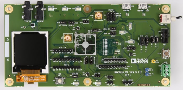
External devices connected to the MAX32690EVKIT:
Bluetooth SMA Connector with a Hinged 2.4GHz Whip Antenna
3-Pin Terminal Block for CAN Bus 2.0
Selectable On-Board High-Precision Voltage Reference
On-Board HyperRAM
Stereo Audio Codec with Line-In and Line-Out 3.5mm Jacks
128 x 128 (1.45in) Color TFT Display
USB 2.0 Micro-B Interface to the MAX32690
USB 2.0 Micro-B to Serial UART
Board Power Provided by either USB Port
Jumpers to Enable Optional Pull-Up Resistors on I2C port
All GPIOs Signals Accessed through 0.1in Headers
Three Analog Inputs Accessed through 0.1in Headers with Optional Filtering
SWD 10-Pin Header
On-Board 3.3V, 1.8V, and 1.1V LDO Regulators
Individual Power Measurement on All IC Rails through Jumpers
Two General-Purpose LEDs and One GeneralPurpose Push Button Switch
Supported Features
The max32690evkit board supports the hardware features listed below.
- on-chip / on-board
- Feature integrated in the SoC / present on the board.
- 2 / 2
-
Number of instances that are enabled / disabled.
Click on the label to see the first instance of this feature in the board/SoC DTS files. -
vnd,foo -
Compatible string for the Devicetree binding matching the feature.
Click on the link to view the binding documentation.
max32690evkit/max32690/m4 target
On-target memory for this board target: 1 MiB of RAM, 3 MiB of Flash.
Type |
Location |
Description |
Compatible |
|---|---|---|---|
CPU |
on-chip |
ARM Cortex-M4F CPU1 |
|
on-chip |
MAX32 RV32 core1 |
||
ADC |
on-chip |
ADI MAX32 ADC SAR1 |
|
CAN |
on-chip |
||
Clock control |
on-chip |
||
on-chip |
MAX32 Global Control1 |
||
Counter |
on-chip |
ADI MAX32 counter6 |
|
on-chip |
ADI MAX32 compatible Counter RTC1 |
||
on-chip |
ADI MAX32 Wake-Up Timer is a unique instance of a 32-bit timer that can wake up the device from sleep, standby and backup modes2 |
||
Display |
on-board |
Sitronix ST7735X display controller1 |
|
DMA |
on-chip |
ADI MAX32 DMA1 |
|
Flash controller |
on-chip |
MAX32XXX flash controller2 |
|
GPIO & Headers |
on-chip |
MAX32 GPIO5 |
|
I2C |
on-chip |
||
Input |
on-board |
Group of GPIO-bound input keys1 |
|
Interrupt controller |
on-chip |
ARMv7-M NVIC (Nested Vectored Interrupt Controller)1 |
|
LED |
on-board |
Group of GPIO-controlled LEDs1 |
|
Mailbox |
on-chip |
ADI MAX32 SEMA Mailbox1 |
|
Memory controller |
on-chip |
MAX32 HyperBus (HPB) Memory Controller Interface1 |
|
MTD |
on-chip |
Flash node2 |
|
Pin control |
on-chip |
MAX32 Pin Controller1 |
|
PWM |
on-chip |
ADI MAX32 PWM4 |
|
QSPI |
on-chip |
MAX32 SPIXF device representation1 |
|
RNG |
on-chip |
ADI MAX32XXX TRNG1 |
|
Serial controller |
on-chip |
||
SPI |
on-chip |
||
SRAM |
on-chip |
Generic on-chip SRAM9 |
|
Timer |
on-chip |
ADI MAX32 timer8 |
|
on-chip |
ARMv7-M System Tick1 |
||
USB |
on-chip |
ADI MAX32 USBHS1 |
|
1-Wire |
on-chip |
ADI MAX32xxx MCUs 1-Wire Master1 |
|
Watchdog |
on-chip |
max32690evkit/max32690/rv32 target
On-target memory for this board target: 128 KiB of RAM, 256 KiB of Flash.
Type |
Location |
Description |
Compatible |
|---|---|---|---|
CPU |
on-chip |
MAX32 RV32 core1 |
|
ADC |
on-chip |
ADI MAX32 ADC SAR1 |
|
CAN |
on-chip |
ADI MAX32 CAN Node2 |
|
Clock control |
on-chip |
||
on-chip |
MAX32 Global Control1 |
||
Counter |
on-chip |
ADI MAX32 counter6 |
|
on-chip |
ADI MAX32 compatible Counter RTC1 |
||
on-chip |
ADI MAX32 Wake-Up Timer is a unique instance of a 32-bit timer that can wake up the device from sleep, standby and backup modes2 |
||
DMA |
on-chip |
ADI MAX32 DMA1 |
|
Flash controller |
on-chip |
||
GPIO & Headers |
on-chip |
MAX32 GPIO5 |
|
I2C |
on-chip |
||
Input |
on-board |
Group of GPIO-bound input keys1 |
|
Interrupt controller |
on-chip |
MAX32 RV32 Core Interrupt Controller1 |
|
LED |
on-board |
Group of GPIO-controlled LEDs1 |
|
Mailbox |
on-chip |
ADI MAX32 SEMA Mailbox1 |
|
MTD |
on-chip |
Flash node2 |
|
Pin control |
on-chip |
MAX32 Pin Controller1 |
|
PWM |
on-chip |
ADI MAX32 PWM4 |
|
RNG |
on-chip |
ADI MAX32XXX TRNG1 |
|
Serial controller |
on-chip |
||
SPI |
on-chip |
ADI MAX32 SPI3 |
|
SRAM |
on-chip |
Generic on-chip SRAM2 |
|
Timer |
on-chip |
ADI MAX32 timer7 |
|
on-chip |
ADI MAX32 RV32 system timer1 |
||
1-Wire |
on-chip |
ADI MAX32xxx MCUs 1-Wire Master1 |
|
Watchdog |
on-chip |
Connections and IOs
Name |
Name |
Settings |
Description |
||||||
|---|---|---|---|---|---|---|---|---|---|
JP1 |
VREF |
|
|
||||||
JP2 |
I2C0 PU |
|
|
||||||
JP3 |
I2C0_SDA_PU |
|
|
||||||
JP4 |
I2C0_SCL_PU |
|
|
||||||
JP5 |
LED0 EN |
|
|
||||||
JP6 |
LED1 EN |
|
|
||||||
JP7 |
RX EN |
|
|
||||||
JP8 |
TX EN |
|
|
||||||
JP9 |
P1_7 SEL |
|
|
||||||
JP10 |
P1_8 SEL |
|
|
||||||
JP11 |
V_AUX SEL |
|
|
||||||
JP12 |
VDD3A EN |
|
|
||||||
JP13 |
VDDIOH EN |
|
|
||||||
JP14 |
VDDB EN |
|
|
||||||
JP15 |
VDDA EN |
|
|
||||||
JP16 |
VDDIO EN |
|
|
||||||
JP17 |
VCORE EN |
|
|
||||||
JP18 |
BLE LDO EN |
|
|
||||||
JH6 |
ANALOG PORT3 |
|
|
Programming and Debugging
The max32690evkit board supports the runners and associated west commands listed below.
| flash | debug | debugserver | attach | rtt | reset | |
|---|---|---|---|---|---|---|
| jlink | ✅ | ✅ | ✅ | ✅ | ✅ | ✅ |
| openocd | ✅ (default) | ✅ (default) | ✅ | ✅ | ✅ |
Flashing
The MAX32690 MCU can be flashed by connecting an external debug probe to the SWD port. SWD debug can be accessed through the Cortex 10-pin connector, J3. Logic levels are fixed to VDDIO (1.8V).
Once the debug probe is connected to your host computer, then you can simply run the
west flash command to write a firmware image into flash. To perform a full erase,
pass the --erase option when executing west flash.
Note
This board uses OpenOCD as the default debug interface. You can also use
a Segger J-Link with Segger’s native tooling by overriding the runner,
appending --runner jlink to your west command(s). The J-Link should
be connected to the standard 2*5 pin debug connector (JW3) using an
appropriate adapter board and cable.
Debugging
Please refer to the Flashing section and run the west debug command
instead of west flash.