SDP-K1
Overview
The EVAL-SDP-CK1Z (SDP-K1) controller board is a system demonstration platform (SDP) from Analog Devices designed to connect to evaluation shields containing ADI components.
STM32 microcontroller in BGA216 package
USB 2.0 device with USB-C connector
USB debug interface supporting CMSIS-DAP through a NXP Freescale microcontroller
Flexible board power supply
USB VBUS 5 V max. 500 mA
5.5mm DC power jack 7 - 12 V min. 300 mA
VIN from Arduino* compatible connectors
VIN from 120-pin connector 5 V min. 300 mA
3 color LEDs (green, orange, red) and 1 status LED
One push-buttons: RESET
16MB SDRAM
Arduino UNO and 120-pin SDP connectors
More information about the board can be found on the ADI SDP-K1 website.
Hardware
ADI SDP-K1 provides the following hardware components:
STM32F469NIH6 in BGA216 package
ARM® 32-bit Cortex®-M4 CPU with FPU
180 MHz max CPU frequency
VDD of 1.8 V or 3.3 V
2 MB Flash
384 KB SRAM
GPIO with external interrupt capability
LCD parallel interface, 8080/6800 modes
LCD TFT controller supporting up to XGA resolution
MIPI® DSI host controller supporting up to 720p 30Hz resolution
3x12-bit ADC with 24 channels
2x12-bit D/A converters
RTC
Advanced-control Timer
General Purpose Timers (17)
Watchdog Timers (2)
USART/UART (8)
I2C (3)
SPI (6)
1xSAI (serial audio interface)
SDIO
2xCAN
USB 2.0 OTG FS with on-chip PHY
USB 2.0 OTG HS/FS with dedicated DMA, on-chip full-speed PHY and ULPI
10/100 Ethernet MAC with dedicated DMA
8- to 14-bit parallel camera
CRC calculation unit
True random number generator
DMA Controller
More information about STM32F469NI can be found here:
Supported Features
The adi_sdp_k1 board supports the hardware features listed below.
- on-chip / on-board
- Feature integrated in the SoC / present on the board.
- 2 / 2
-
Number of instances that are enabled / disabled.
Click on the label to see the first instance of this feature in the board/SoC DTS files. -
vnd,foo -
Compatible string for the Devicetree binding matching the feature.
Click on the link to view the binding documentation.
adi_sdp_k1/stm32f469xx target
On-target memory for this board target: 320 KiB of RAM, 2 MiB of Flash.
Type |
Location |
Description |
Compatible |
|---|---|---|---|
CPU |
on-chip |
ARM Cortex-M4F CPU1 |
|
ADC |
on-chip |
STM32F4 ADC3 |
|
CAN |
on-chip |
STM32 CAN controller2 |
|
Clock control |
on-chip |
STM32F4 RCC (Reset and Clock controller)1 |
|
on-chip |
STM32 HSE Clock1 |
||
on-chip |
|||
on-chip |
|||
on-chip |
STM32 Clock multiplexer1 |
||
on-chip |
STM32 Microcontroller Clock Output (MCO)2 |
||
Counter |
on-chip |
STM32 counters14 |
|
DAC |
on-chip |
STM32 family DAC1 |
|
Display |
on-chip |
STM32 LCD-TFT display controller1 |
|
DMA |
on-chip |
STM32 DMA controller (V1)2 |
|
Ethernet |
on-chip |
ST STM32 Ethernet MAC, a child node of the Ethernet controller1 |
|
on-chip |
STM32 MDIO Controller1 |
||
Flash controller |
on-chip |
STM32 Family flash controller1 |
|
GPIO & Headers |
on-chip |
STM32 GPIO Controller11 |
|
on-board |
GPIO pins exposed on Arduino Uno (R3) headers1 |
||
on-board |
GPIO pins exposed on a Analog devices SDP interface1 |
||
on-board |
GPIO pins exposed on a Digilent Pmod interface2 |
||
I2C |
on-chip |
STM32 I2C V1 controller3 |
|
I2S |
on-chip |
STM32 I2S controller2 |
|
on-chip |
STM32 SAI Block controller1 |
||
Interrupt controller |
on-chip |
ARMv7-M NVIC (Nested Vectored Interrupt Controller)1 |
|
on-chip |
STM32 External Interrupt Controller1 |
||
LED |
on-board |
Group of GPIO-controlled LEDs1 |
|
Memory controller |
on-chip |
STM32 Battery Backed RAM1 |
|
on-chip |
STM32 Flexible Memory Controller (FMC)1 |
||
on-chip |
STM32 Flexible Memory Controller (SDRAM controller)1 |
||
MIPI-DSI |
on-chip |
STM32 MIPI DSI host1 |
|
MMC |
on-chip |
STM32 SDMMC Host Controller1 |
|
MTD |
on-chip |
STM32F4 flash memory1 |
|
NVMEM |
on-chip |
Fixed layout for Non-Volatile memory1 |
|
OTP memory |
on-chip |
||
PHY |
on-chip |
This binding is to be used by all the usb transceivers which are built-in with USB IP2 |
|
on-board |
This binding is to be used by all the usb transceivers which are an external ULPI phy1 |
||
Pin control |
on-chip |
STM32 Pin controller1 |
|
Power management |
on-chip |
STM32 power controller1 |
|
PWM |
on-chip |
STM32 PWM12 |
|
Reset controller |
on-chip |
STM32 Reset and Clock Control (RCC) Controller1 |
|
RNG |
on-chip |
STM32 Random Number Generator1 |
|
RTC |
on-chip |
STM32 RTC1 |
|
Sensors |
on-chip |
STM32 quadrature decoder6 |
|
on-chip |
STM32 family TEMP node for production calibrated sensors with two calibration temperatures1 |
||
on-chip |
STM32 VREF+1 |
||
on-chip |
STM32 VBAT1 |
||
Serial controller |
on-chip |
STM32 USART4 |
|
on-chip |
|||
SMbus |
on-chip |
STM32 SMBus controller3 |
|
SPI |
on-chip |
||
Timer |
on-chip |
ARMv7-M System Tick1 |
|
on-chip |
STM32 timers14 |
||
USB |
on-chip |
STM32 OTGFS controller1 |
|
on-chip |
STM32 OTGHS controller1 |
||
Watchdog |
on-chip |
STM32 watchdog1 |
|
on-chip |
STM32 system window watchdog1 |
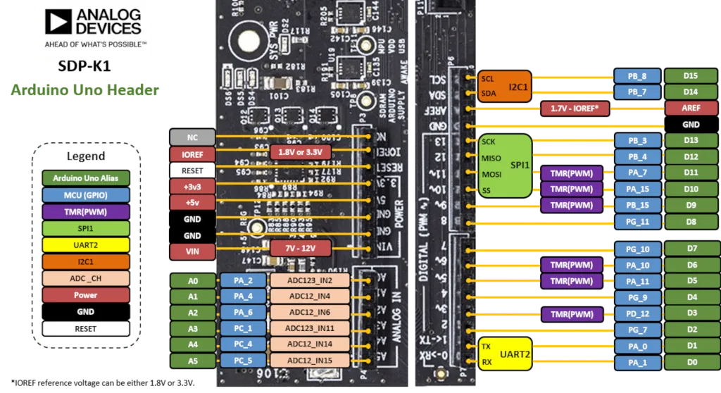
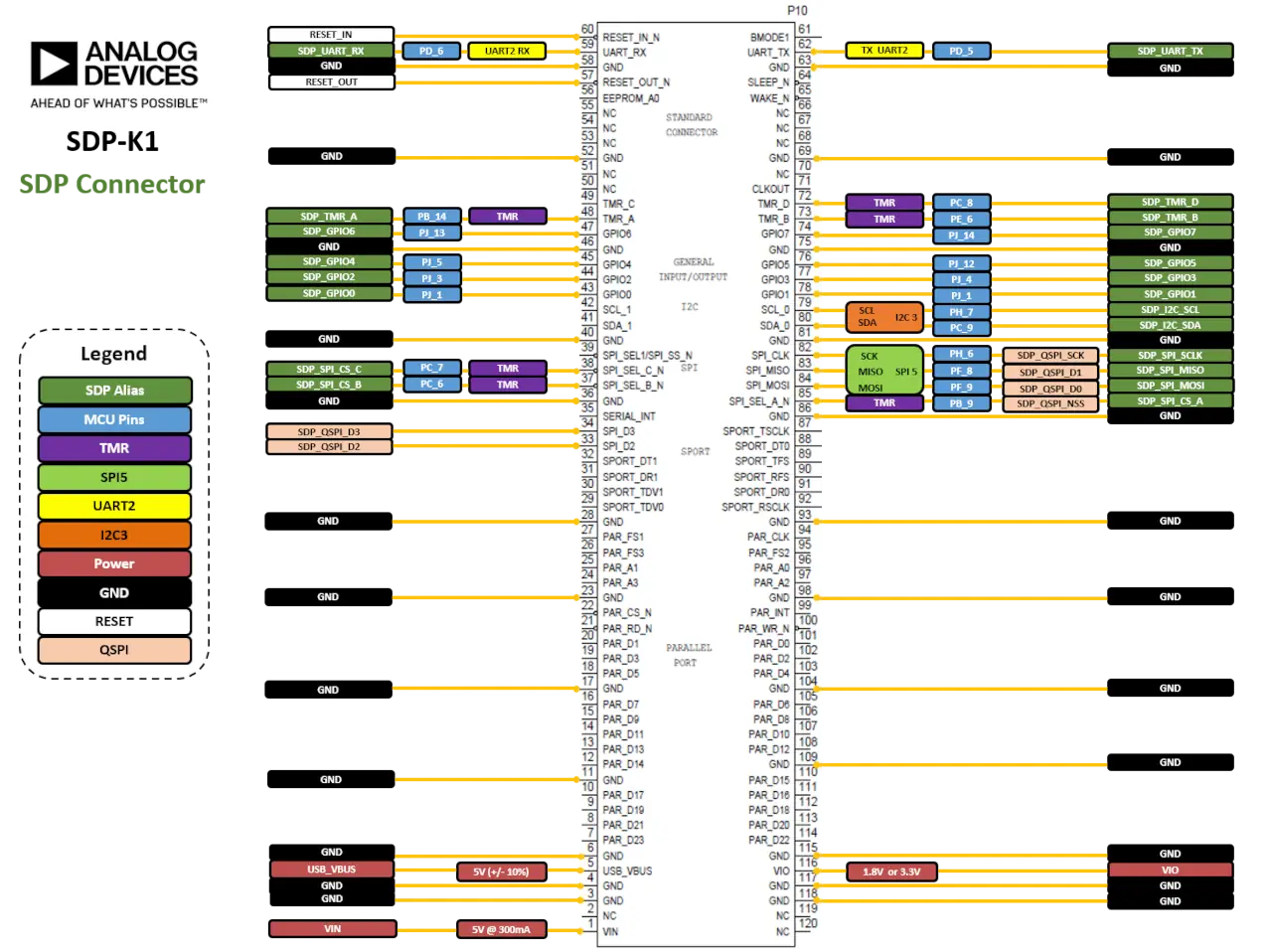
Pin Mapping
For more details please refer to EVAL-SDP-CK1Z User Guide.
Arduino UNO headers
120-pin SDP connector
Default Zephyr Peripheral Mapping:
UART_5 TX/RX : P2 (DAPLink USB-C)
UART_5 TX/RX : P8 (DAPLink two position through hole)
LED1 : DS6 (Red)
LED2 : DS5 (Orange)
LED3 : DS4 (Green)
LED4 : DS4 (Status)
Programming and Debugging
The adi_sdp_k1 board supports the runners and associated west commands listed below.
| flash | debug | debugserver | attach | rtt | reset | |
|---|---|---|---|---|---|---|
| jlink | ✅ | ✅ | ✅ | ✅ | ✅ | ✅ |
| openocd | ✅ (default) | ✅ (default) | ✅ | ✅ | ✅ |
The ADI SDP-K1 be programmed over USB using the DAPLink firmware running on an
embedded NXP Freescale microcontroller or a 10-pin DEBUG header connected
to a STLINK debugger.
DAPLink exposes a storage device, as well as USB HID and CDC Endpoints, to the host. For more details please refer to the Official DAPLink website.
Flashing
Flashing an application with a STLINK debugger
First, connect the STLINK debugger to your host computer using the Micro-USB port.
Then attach the debugger to the 10-pin DEBUG header on the SDP-K1. Finally
connect the SDP-K1 to your host computer using the USB-C port.
Run a serial host program to connect with your board:
$ minicom -D /dev/serial/by-id/usb-ARM_DAPLink_CMSIS-DAP_<...>
Here is an example for the Hello World application.
# From the root of the zephyr repository
west build -b adi_sdp_k1 samples/hello_world
west flash
You should see the following message on the console:
Hello World! adi_sdp_k1