BLE400
Overview
BLE400 is a motherboard designed for BLE Bluetooth 2.4G Wireless Module. Used together with core board – Core51822.
Hardware
Motherboard
Onboard battery holder, multi power supplies are available
All the IOs are accessible for easy expansion
Integrates CP2102 for debugging
LEDs and user keys, compatible with other official boards, easy to use
Core board
Onboard chip: nRF51822
Communication distance (open outdoor 1M data rate): 30m
Frequency range: 2.4GHz
Operating voltage: 2.0V ~ 3.6V
Operating temperature: -40℃ ~ 85℃
Expansion pinheader: all the I/Os except P0.26 and P0.27
Pinheader pitch: 2.00mm
Antenna: onboard antenna
Supported Features
The nrf51_ble400 board supports the hardware features listed below.
- on-chip / on-board
- Feature integrated in the SoC / present on the board.
- 2 / 2
-
Number of instances that are enabled / disabled.
Click on the label to see the first instance of this feature in the board/SoC DTS files. -
vnd,foo -
Compatible string for the Devicetree binding matching the feature.
Click on the link to view the binding documentation.
nrf51_ble400/nrf51822 target
On-target memory for this board target: 32 KiB of RAM, 256 KiB of Flash.
Type |
Location |
Description |
Compatible |
|---|---|---|---|
CPU |
on-chip |
ARM Cortex-M0 CPU1 |
|
ADC |
on-chip |
nRF ADC node1 |
|
ARM architecture |
on-chip |
Nordic UICR (User Information Configuration Registers)1 |
|
on-chip |
Nordic nRF family MPU (Memory Protection Unit)1 |
||
on-chip |
Nordic nRF family SWI (Software Interrupt)6 |
||
Clock control |
on-chip |
Nordic nRF clock control node1 |
|
on-chip |
Nordic nRF high-frequency crystal oscillator (nRF51 series)1 |
||
Comparator |
on-chip |
Nordic nRF LPCOMP (analog Low-Power COMParator)1 |
|
Counter |
on-chip |
Nordic nRF timer node3 |
|
Cryptographic accelerator |
on-chip |
Nordic ECB (AES electronic codebook mode encryption)1 |
|
on-chip |
Nordic nRF family CCM (AES CCM mode encryption)1 |
||
Flash controller |
on-chip |
Nordic NVMC (Non-Volatile Memory Controller)1 |
|
GPIO & Headers |
on-chip |
NRF5 GPIOTE1 |
|
on-chip |
NRF5 GPIO1 |
||
I2C |
on-chip |
||
Input |
on-board |
Group of GPIO-bound input keys1 |
|
Interrupt controller |
on-chip |
ARMv6-M NVIC (Nested Vectored Interrupt Controller) controller1 |
|
LED |
on-board |
Group of GPIO-controlled LEDs1 |
|
Miscellaneous |
on-chip |
Nordic FICR (Factory Information Configuration Registers)1 |
|
on-chip |
Nordic nRF family PPI (Programmable Peripheral Interconnect)1 |
||
MTD |
on-chip |
Flash node1 |
|
Networking |
on-chip |
Nordic nRF family RADIO peripheral1 |
|
Pin control |
on-chip |
Nordic nRF family Pin Controller1 |
|
Power management |
on-chip |
Nordic nRF power control node1 |
|
PWM |
on-chip |
nRFx S/W PWM1 |
|
Retained memory |
on-chip |
Nordic GPREGRET (General Purpose Register Retention) device1 |
|
RNG |
on-chip |
Nordic nRF family RNG (Random Number Generator)1 |
|
RTC |
on-chip |
Nordic nRF RTC (Real-Time Counter)2 |
|
Sensors |
on-chip |
Nordic nRF family TEMP node1 |
|
on-chip |
Nordic nRF quadrature decoder (QDEC) node1 |
||
Serial controller |
on-chip |
Nordic nRF family UART1 |
|
SPI |
on-chip |
||
SRAM |
on-chip |
Generic on-chip SRAM1 |
|
Watchdog |
on-chip |
Nordic nRF family WDT (Watchdog Timer)1 |
Features
2.4 GHz multiprotocol RF transceiver
ARM® Cortex®-M0 32 bit processor
128 bit AES HW encryption
256kB flash & 32kB RAM
Programmable Peripheral Interconnect (PPI)
Digital interfaces: SPI, I2C, UART
10 bit ADC
Programmable output power: -20 to +4 dBm
Independent application development and protocol stack
Fully compatible with NRF24L series
Pinout compatible with NRF51xxx series
Global separate power management
Operating voltage: 1.8 V ~ 3.6 V
Revision History
Core board
In June of 2015, Core51822 and its variant, Core51822 (B), upgraded the onboard chip to Rev3 (nRF51822_QFAC) that features 32kB RAM.
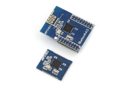
Top: Core51822 Bottom: Core51822 (B)
Connections and IOs
Motherboard
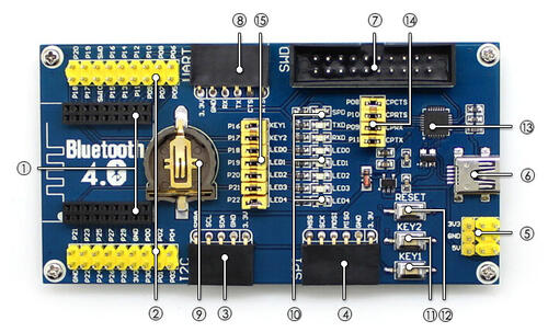
Wireless module connector: for easily connecting modules like Core51822
MCU pins expansion connector
I2C interface
SPI interface
5V/3.3V power input/output: usually used as power output, also common-grounding with other user board
USB connector: USB TO UART via onboard converter CP2102
Debugging interface
UART interface
Battery holder
User LEDs
User keys
Reset button
CP2102
USB TO UART jumper
LEDs & Keys jumper
Core board
BLE400 dimensions

Connections and IOs
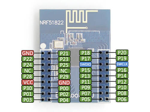
LED
LED0 (red) = P0.18
LED1 (red) = P0.19
LED2 (red) = P0.20
LED3 (red) = P0.21
LED4 (red) = P0.22
SUSPEND = SUSPEND
RXD1 = P0.9
TXD1 = P0.11
I2C
SMBA = P0.02
SCL = P0.01
SDA = P0.00
SPI
NSS = P0.30
SCK = P0.25
MOSI = P0.24
MISO = P0.23
USART1
RX = P0.05
TX = P0.06
CTS = P0.07
RTS = P0.12
UART (USB)
RX = P0.9
TX = P0.11
CTS = P0.8
RTS = P0.10
Programming and Debugging
The nrf51_ble400 board supports the runners and associated west commands listed below.
| flash | debug | reset | rtt | attach | debugserver | |
|---|---|---|---|---|---|---|
| jlink | ✅ | ✅ (default) | ✅ | ✅ | ✅ | ✅ |
| nrfjprog | ✅ | |||||
| nrfutil | ✅ (default) |
Flashing
Follow the instructions in the Nordic nRF5x Segger J-Link page to install and configure all the necessary software. Further information can be found in Flashing. Then build and flash applications as usual (see Building an Application and Run an Application for more details).
Here is an example for the Hello World application.
First, run your favorite terminal program to listen for output.
$ minicom -D <tty_device> -b 115200
Replace <tty_device> with the port where the board nRF51 DK
can be found. For example, under Linux, /dev/ttyACM0.
Then build and flash the application in the usual way.
# From the root of the zephyr repository
west build -b nrf51_ble400 samples/hello_world
west flash
Debugging
Refer to the Nordic nRF5x Segger J-Link page to learn about debugging Nordic boards with a Segger IC.