FK7B0M1-VBT6
FANKE FK7B0M1-VBT6
Overview
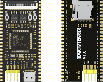
The FK7B0M1-VBT6 core board by FANKE Technology Co., Ltd. is an advanced microcontroller platform based on the STMicroelectronics Arm® Cortex®-M7 core STM32H7B0VBT6 microcontroller. This board is an ideal solution for developers looking to create high-performance applications, especially in the field of Human-Machine Interface (HMI), leveraging its robust capabilities and support for sophisticated display and touch technologies.
The FK7B0M1-VBT6 is designed as a reference design for user application development before transitioning to the final product, significantly simplifying the development process. Its wide range of hardware features, including advanced display and touch capabilities, make it exceptionally suitable for HMI applications, allowing for comprehensive evaluation and testing of peripherals and functionalities.

Hardware
FK7B0M1-VBT6 provides the following hardware components:
STM32H7B6VB in LQFP100 package
ARM 32-bit Cortex-M7 CPU with FPU
280 MHz max CPU frequency
VDD from 1.62 V to 3.6 V
128 KB Flash
~1.4 MB SRAM max (1.18 Mbytes user SRAM + 64 Kbytes ITCM RAM + 128 Kbytes DTCM RAM + 4 Kbytes SRAM in Backup domain)
Main clock: External 25MHz crystal oscillator.
RTC: 32.768kHz crystal oscillator.
32-bit timers(2)
16-bit timers(12)
1 reset button, 1 user button, and 1 BOOT button
1 user LED
External 64-Mbit QSPI (W25Q64) NOR Flash memory.
External 64-Mbit SPI (W25Q64) NOR Flash memory.
USB OTG Full Speed and High Speed(1)
1 micro SD card
1 RGB LCD interface
SWD and serial port accessibility through a pin header
Bring out 39 IO ports
More information about STM32H7B0VB can be found here:
Supported Features
The fk7b0m1_vbt6 board supports the hardware features listed below.
- on-chip / on-board
- Feature integrated in the SoC / present on the board.
- 2 / 2
-
Number of instances that are enabled / disabled.
Click on the label to see the first instance of this feature in the board/SoC DTS files. -
vnd,foo -
Compatible string for the Devicetree binding matching the feature.
Click on the link to view the binding documentation.
fk7b0m1_vbt6/stm32h7b0xx target
On-target memory for this board target: 256 KiB of RAM, 128 KiB of Flash.
Type |
Location |
Description |
Compatible |
|---|---|---|---|
CPU |
on-chip |
ARM Cortex-M7 CPU1 |
|
ADC |
on-chip |
STM32 ADC3 |
|
Audio |
on-chip |
STMicroelectronics DFSDM block1 |
|
on-chip |
STMicroelectronics DFSDM DMIC8 |
||
CAN |
on-chip |
STM32H7 series (and compatible) FDCAN CAN FD controller2 |
|
Clock control |
on-chip |
STM32H7 RCC (Reset and Clock controller)1 |
|
on-chip |
STM32 HSE Clock1 |
||
on-chip |
STM32 HSI Clock1 |
||
on-chip |
|||
on-chip |
STM32 LSE Clock1 |
||
on-chip |
|||
on-chip |
STM32 Clock multiplexer1 |
||
on-chip |
STM32 Microcontroller Clock Output (MCO)2 |
||
Comparator |
on-chip |
STM32H7 series Comparator2 |
|
Counter |
on-chip |
STM32 counters14 |
|
CRC |
on-chip |
STM32 CRC calculation unit1 |
|
Cryptographic accelerator |
on-chip |
STM32 Cryptographic Accelerator1 |
|
on-chip |
STM32 HASH Processor1 |
||
DAC |
on-chip |
STM32 family DAC1 |
|
Display |
on-chip |
STM32 LCD-TFT display controller1 |
|
DMA |
on-chip |
STM32 DMA controller (V1)2 |
|
on-chip |
STM32 BDMA controller1 |
||
on-chip |
STM32 DMAMUX controller2 |
||
Ethernet |
on-chip |
STM32H7 Ethernet1 |
|
on-chip |
STM32 MDIO Controller1 |
||
Flash controller |
on-chip |
STM32 Family flash controller1 |
|
on-board |
STM32 OSPI Flash controller supporting the JEDEC CFI interface1 |
||
GPIO & Headers |
on-chip |
STM32 GPIO Controller11 |
|
I2C |
on-chip |
STM32 I2C V2 controller4 |
|
I2S |
on-chip |
STM32H7 I2S controller4 |
|
on-chip |
STM32 SAI Block controller1 |
||
Input |
on-board |
Group of GPIO-bound input keys1 |
|
Interrupt controller |
on-chip |
ARMv7-M NVIC (Nested Vectored Interrupt Controller)1 |
|
on-chip |
STM32 External Interrupt Controller1 |
||
LED |
on-board |
Group of GPIO-controlled LEDs1 |
|
Memory controller |
on-chip |
STM32H7 Flexible Memory Controller (FMC)1 |
|
on-chip |
STM32 Flexible Memory Controller (SDRAM controller)1 |
||
MMC |
on-chip |
STM32 SDMMC Host Controller2 |
|
MMU / MPU |
on-chip |
ARMv7-M Memory Protection Unit (MPU)1 |
|
MTD |
on-chip |
STM32 flash memory1 |
|
on-board |
Properties supporting Zephyr spi-nor flash driver (over the Zephyr SPI API) control of serial flash memories using the standard M25P80-based command set1 |
||
on-board |
Fixed partitions of a flash (or other non-volatile storage) memory2 |
||
NVMEM |
on-chip |
Fixed layout for Non-Volatile memory1 |
|
OCTOSPI |
on-chip |
||
OTP memory |
on-chip |
STM32 embedded NVM OTP1 |
|
PHY |
on-chip |
This binding is to be used by all the usb transceivers which are built-in with USB IP1 |
|
Pin control |
on-chip |
STM32 Pin controller1 |
|
Power management |
on-chip |
STM32H7 power controller1 |
|
PWM |
on-chip |
STM32 PWM12 |
|
Reset controller |
on-chip |
STM32 Reset and Clock Control (RCC) Controller1 |
|
RNG |
on-chip |
STM32 Random Number Generator1 |
|
RTC |
on-chip |
STM32 RTC1 |
|
Sensors |
on-chip |
STM32 quadrature decoder6 |
|
on-chip |
STM32 Digital Temperature Sensor1 |
||
on-chip |
STM32 family TEMP node for production calibrated sensors with two calibration temperatures1 |
||
on-chip |
STM32 VBAT1 |
||
on-chip |
STM32 VREF+1 |
||
Serial controller |
on-chip |
||
on-chip |
STM32 UART4 |
||
on-chip |
STM32 LPUART1 |
||
SMbus |
on-chip |
STM32 SMBus controller4 |
|
SPI |
on-chip |
||
Timer |
on-chip |
ARMv7-M System Tick1 |
|
on-chip |
STM32 timers14 |
||
on-chip |
STM32 low-power timer (LPTIM)1 |
||
USB |
on-chip |
STM32 OTGHS controller1 |
|
Video |
on-chip |
STM32 DCMI1 |
|
on-chip |
STM32 JPEG HW Codec1 |
||
Watchdog |
on-chip |
STM32 watchdog1 |
|
on-chip |
STM32 system window watchdog1 |
Pin Mapping
FK7B0M1-VBT6 board has 5 GPIO controllers. These controllers are responsible for pin muxing, input/output, pull-up, etc.
Default Zephyr Peripheral Mapping:
The FK7B0M1-VBT6 board is configured as follows
UART_1 TX/RX : PA9/PA10 (available on the header pins)
User LED (blue) : PC1
User PB : PC13
SPI1 NCS/CLK/MISO/MOSI : PA15/PB3/PB4/PB5 (NOR Flash)
QuadSPI NCS/CLK/IO0/IO1/IO2/IO3 : PB6/PB2/PD11/PD12/PE2/PD13 (NOR Flash)
USB DM/DP : PA11/PA12
System Clock
The FK7B0M1-VBT6 System Clock could be driven by an internal or external oscillator, as well as by the main PLL clock. By default the system clock is driven by the PLL clock at 280MHz, driven by an 25MHz external crystal oscillator.
Serial Port
The Zephyr console output is assigned to UART1. The default communication settings are 115200 8N1.
Programming and Debugging
Applications for the fk7b0m1_vbt6 board configuration can be built and flashed in the usual
way (see Building an Application and Run an Application for more details).
Flashing
The FK7B0M1-VBT6 board does not include an on-board debugger. As a result, it requires an external debugger, such as ST-Link, for programming and debugging purposes.
The board provides header pins for the Serial Wire Debug (SWD) interface.
Flashing an application to FK7B0M1-VBT6
To begin, connect the ST-Link Debug Programmer to the FK7B0M1-VBT6 board using the SWD interface. Next, connect the ST-Link to your host computer via a USB port. Once this setup is complete, you can proceed to build and flash your application to the board
Here is an example for the Hello World application.
# From the root of the zephyr repository
west build -b fk7b0m1_vbt6 samples/hello_world
west flash
Run a serial host program to connect with your board:
$ minicom -D /dev/ttyACM0 -b 115200
Then, press the RESET button, you should see the following message:
Hello World! fk7b0m1_vbt6
Debugging
This current Zephyr port does not support debugging.