RA2A1 Evaluation Kit
Overview
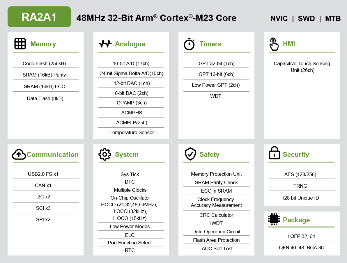
The EK-RA2A1 is an evaluation kit for Renesas RA2A1 Microcontroller Group.
Renesas RA2A1 Microcontroller Group has following features
48MHz, Arm Cortex-M23 core
256kB Code Flash, 8kB Data Flash, 32kB SRAM
USB 2.0 Full-Sppeed
SCI x 3
SPI x 2
I2C x 2
CAN x 1
16-bit A/D Converter
24-bit Sigma-Delta A/D Converter
12-bit D/A Converter
8-bit D/A Converter x 2
High-Speed Analog Comparator
Low-Power Analog Comparator
OPAMP x 3
Temperature Sensor
General PWM Timer 32-bit x 1
General PWM Timer 16-bit x 6
Low Power Asynchronous General-Purpose Timer x 2
Watchdog Timer
49 Input/Output pins
Hardware
Detail Hardware feature for the RA2A1 MCU group can be found at RA2A1 Group User’s Manual Hardware [1]
RA2A1 Block diagram (Credit: Renesas Electronics Corporation)
Detail Hardware feature for the EK-RA2A1 MCU can be found at EK-RA2A1 - User’s Manual [1]
EK-RA2A1 has following features.
Native pin access through 4x 40-pin male headers
MCU current measurement points
SEGGER J-Link on-board programmer and debugger
Two Digilent Pmod (SPI and UART)
User LED
Mechanical user button
Capacitive user button
Supported Features
The ek_ra2a1 board supports the hardware features listed below.
- on-chip / on-board
- Feature integrated in the SoC / present on the board.
- 2 / 2
-
Number of instances that are enabled / disabled.
Click on the label to see the first instance of this feature in the board/SoC DTS files. -
vnd,foo -
Compatible string for the Devicetree binding matching the feature.
Click on the link to view the binding documentation.
ek_ra2a1/r7fa2a1ab3cfm target
On-target memory for this board target: 32 KiB of RAM, 256 KiB of Flash.
Type |
Location |
Description |
Compatible |
|---|---|---|---|
CPU |
on-chip |
ARM Cortex-M23 CPU1 |
|
ADC |
on-chip |
Renesas RA 16-bit resolution ADC (ADC16)1 |
|
Clock control |
on-chip |
Renesas RA Clock Generation Circuit external clock configuration1 |
|
on-chip |
Generic fixed-rate clock provider3 |
||
on-chip |
Renesas RA Sub-Clock1 |
||
on-chip |
Renesas RA Clock Control node pclk block1 |
||
on-chip |
|||
Counter |
on-chip |
Renesas RA AGT as Counter2 |
|
CRC |
on-chip |
Renesas RA CRC device1 |
|
DAC |
on-chip |
Renesas RA DAC Controller Global1 |
|
on-chip |
Renesas RA DAC Controller1 |
||
Flash controller |
on-chip |
Renesas RA family flash low-power controller1 |
|
GPIO & Headers |
on-chip |
||
I2C |
on-chip |
Renesas RA SCI I2C controller3 |
|
on-chip |
|||
Input |
on-chip |
Renesas RA Capacitive Sensing Unit1 |
|
on-board |
Renesas RA Capacitive Touch Button instance1 |
||
on-board |
Group of GPIO-bound input keys1 |
||
Interrupt controller |
on-chip |
ARMv8-M NVIC (Nested Vectored Interrupt Controller)1 |
|
LED |
on-board |
Group of GPIO-controlled LEDs1 |
|
Miscellaneous |
on-chip |
Renesas RA Event Link Controller1 |
|
on-chip |
|||
on-chip |
Renesas RA AGT2 |
||
on-chip |
|||
MTD |
on-chip |
Flash memory binding for Renesas RA Code flash region1 |
|
on-chip |
Flash memory binding for Renesas RA Data flash region1 |
||
on-board |
Fixed partitions of a flash (or other non-volatile storage) memory1 |
||
Pin control |
on-chip |
Renesas RA Pin Controller1 |
|
PWM |
on-chip |
||
Reserved memory |
on-chip |
Renesas Option-Setting Memory3 |
|
RNG |
on-chip |
Renesas RA TRNG1 |
|
Serial controller |
on-chip |
||
SPI |
on-chip |
Renesas RA SCI SPI controller3 |
|
on-chip |
|||
SRAM |
on-chip |
Generic on-chip SRAM1 |
|
Timer |
on-chip |
ARMv8-M System Tick1 |
|
Watchdog |
on-chip |
Renesas RA Watchdog (wdt)1 |
Programming and debugging
The ek_ra2a1 board supports the runners and associated west commands listed below.
| flash | debug | attach | rtt | debugserver | reset | |
|---|---|---|---|---|---|---|
| jlink | ✅ (default) | ✅ (default) | ✅ | ✅ | ✅ | ✅ |
| pyocd | ✅ | ✅ | ✅ | ✅ | ✅ |
Building & Flashing
You can build and flash an application with onboard J-Link debug adapter. Building an Application and Run an Application for more details.
Here is an example for building and flashing the Blinky application.
# From the root of the zephyr repository
west build -b ek_ra2a1 samples/basic/blinky
west flash
Debugging
Debugging also can be done with onboard J-Link debug adapter. The following command is debugging the Blinky application. Also, see the instructions specific to the debug server that you use.
# From the root of the zephyr repository
west build -b ek_ra2a1 samples/basic/blinky
west debug