RA8M1 Evaluation Kit
Overview
The EK-RA8M1 is an Evaluation Kit for Renesas RA8M1 MCU Group which is the first 32-bits MCUs based on new Arm Cortex-M85. The kit offer multiple external interface and peripherals set optimized on board allows user to seamlessly evaluate the features of the RA8M1 MCU and develop embedded system application in various field.
The key features of the EK-RA8M1 board are categorized in three groups as follow:
MCU Native Pin Access
480MHz Arm Cortex-M85 based RA8M1 MCU in 224 pins, BGA package
Native pin access through 2 x 50-pin, and 2 x 40-pin male headers
MCU current measurement points for precision current consumption measurement
Multiple clock sources - RA8M1 MCU oscillator and sub-clock oscillator crystals, providing precision 20.000MHz and 32,768 Hz refeence clocks. Additional low precision clocks are available internal to the RA8M1 MCU
System Control and Ecosystem Access
USB Full Speed Host and Device (micro-AB connector)
Four 5V input sources
USB (Debug, Full Speed, High Speed)
External power supply (using surface mount clamp test points and power input vias)
Three Debug modes
Debug on-board (SWD)
Debug in (ETM, SWD and JTAG)
Debug out (SWD)
User LEDs and buttons
Three User LEDs (red, blue, green)
Power LED (white) indicating availability of regulated power
Debug LED (yellow) indicating the debug connection
Two User buttons
One Reset button
Five most popular ecosystems expansions
Two Seeed Grove system (I2C/I3C) connectors
One SparkFun Qwiic connector
Two Digilent Pmod (SPI, UART and I2C/I3C) connectors
Arduino (Uno R3) connector
MikroElektronika mikroBUS connector
MCU boot configuration jumper
Special Feature Access
Ethernet (RJ45 RMII interface)
USB High Speed Host and Device (micro-AB connector)
512 Mb (64 MB) External Octo-SPI Flash (present in the MCU Native Pin Access area of the EK-RA8M1 board)
CAN FD (3-pin header)
Hardware
Detailed Hardware features for the RA8M1 MCU group can be found at RA8M1 Group User’s Manual Hardware
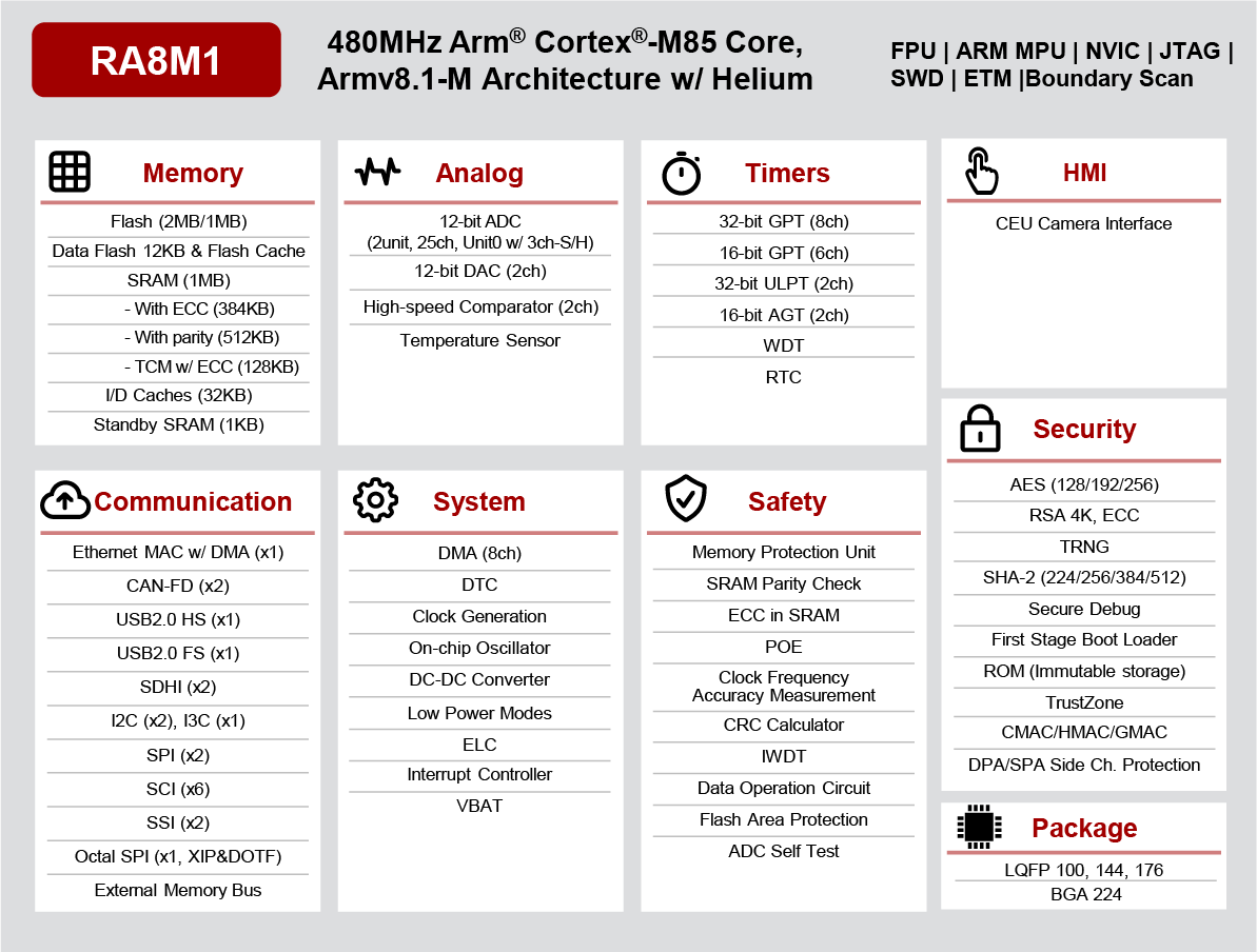
RA8M1 Block diagram (Credit: Renesas Electronics Corporation)
Detailed Hardware features for the EK-RA8M1 MCU can be found at EK-RA8M1 - User’s Manual
Supported Features
The ek_ra8m1 board supports the hardware features listed below.
- on-chip / on-board
- Feature integrated in the SoC / present on the board.
- 2 / 2
-
Number of instances that are enabled / disabled.
Click on the label to see the first instance of this feature in the board/SoC DTS files. -
vnd,foo -
Compatible string for the Devicetree binding matching the feature.
Click on the link to view the binding documentation.
ek_ra8m1/r7fa8m1ahecbd target
On-target memory for this board target: 896 KiB of RAM, 2016 KiB of Flash.
Type |
Location |
Description |
Compatible |
|---|---|---|---|
CPU |
on-chip |
ARM Cortex-M85 CPU1 |
|
ADC |
on-chip |
||
CAN |
on-chip |
Renesas RA CANFD controller global1 |
|
on-chip |
|||
Clock control |
on-chip |
Renesas RA Clock Generation Circuit external clock configuration1 |
|
on-chip |
Generic fixed-rate clock provider3 |
||
on-chip |
Renesas RA Sub-Clock1 |
||
on-chip |
Renesas RA Clock Generation Circuit PLL Clock2 |
||
on-chip |
|||
on-chip |
Renesas RA Clock Control node pclk block1 |
||
on-chip |
|||
on-chip |
Renesas RA External Bus Clock1 |
||
Comparator |
on-chip |
Renesas RA ACMPHS (High-Speed Analog COMParator) Global1 |
|
on-chip |
Renesas RA ACMPHS (High-Speed Analog COMParator) Controller2 |
||
on-chip |
Renesas RA LVD (Low-voltage detection) Controller2 |
||
Counter |
on-chip |
Renesas RA AGT as Counter2 |
|
CRC |
on-chip |
Renesas RA CRC device1 |
|
DAC |
on-chip |
Renesas RA DAC Controller Global1 |
|
on-chip |
|||
DMA |
on-chip |
Renesas RA DMA Controller1 |
|
Ethernet |
on-chip |
Renesas RA Ethernet1 |
|
on-chip |
Renesas RA External MDIO controller1 |
||
on-board |
Generic MII PHY1 |
||
Flash controller |
on-chip |
Renesas RA family flash high-performance controller1 |
|
on-board |
Renesas RA OSPI FLASH1 |
||
GPIO & Headers |
on-chip |
Renesas RA GPIO I/O Port12 |
|
on-board |
GPIO pins exposed on Mikro BUS headers1 |
||
on-board |
GPIO pins exposed on a Digilent Pmod interface2 |
||
I2C |
on-chip |
Renesas RA I2C controller2 |
|
on-chip |
Renesas RA SCI-B I2C controller6 |
||
I2S |
on-chip |
Renesas RA I2S controller2 |
|
I3C |
on-chip |
Renesas RA I3C controller1 |
|
Input |
on-board |
Group of GPIO-bound input keys1 |
|
Interrupt controller |
on-chip |
ARMv8.1-M NVIC (Nested Vectored Interrupt Controller)1 |
|
LED |
on-board |
Group of GPIO-controlled LEDs1 |
|
Memory controller |
on-chip |
Renesas RA SDRAM controller1 |
|
Miscellaneous |
on-chip |
Renesas RA Event Link Controller1 |
|
on-chip |
|||
on-chip |
Renesas RA ULPT2 |
||
on-chip |
Renesas RA AGT2 |
||
on-chip |
|||
MMU / MPU |
on-chip |
ARMv8.1-M MPU (Memory Protection Unit)1 |
|
MTD |
on-chip |
Flash memory binding for Renesas RA Code flash region1 |
|
on-chip |
Flash memory binding for Renesas RA Data flash region1 |
||
on-board |
Fixed partitions of a flash (or other non-volatile storage) memory2 |
||
OCTOSPI |
on-chip |
Renesas RA OSPI1 |
|
PHY |
on-chip |
This binding is to be used by all the usb transceivers which are built-in with USB IP1 |
|
on-chip |
Renesas RA USBHS internal PHY controller1 |
||
on-board |
Simple GPIO controlled CAN transceiver1 |
||
Pin control |
on-chip |
Renesas RA Pin Controller1 |
|
Power management |
on-chip |
Renesas RA battery backup domain1 |
|
PWM |
on-chip |
||
RNG |
on-chip |
Renesas RA RSIP-E51A TRNG1 |
|
RTC |
on-chip |
Renesas RA RTC1 |
|
SDHC |
on-chip |
Renesas RA SDHC2 |
|
Serial controller |
on-chip |
||
SPI |
on-chip |
Renesas RA SCI B SPI6 |
|
on-chip |
|||
SRAM |
on-chip |
Generic on-chip SRAM1 |
|
Timer |
on-chip |
ARMv8.1-M System Tick1 |
|
on-chip |
Renesas RA ULPT TIMER2 |
||
USB |
on-chip |
Renesas RA USB full-speed controller1 |
|
on-chip |
|||
on-chip |
Renesas RA USB high-speed controller1 |
||
Video |
on-chip |
Renesas RA Capture Engine Unit Driver (ceu)1 |
|
Watchdog |
on-chip |
Renesas RA Watchdog (wdt)1 |
Note
For using Ethernet module on EK-RA8M1, remove jumper J61 to enable Ethernet B
For using SDHC driver on EK-RA8M1, remove jumper J61 to use with channel 0
For using I3C driver on EK-RA8M1, install jumper J61 to use with channel 0
Programming and Debugging
The ek_ra8m1 board supports the runners and associated west commands listed below.
| flash | debug | attach | rtt | debugserver | reset | |
|---|---|---|---|---|---|---|
| jlink | ✅ (default) | ✅ (default) | ✅ | ✅ | ✅ | ✅ |
| pyocd | ✅ | ✅ | ✅ | ✅ | ✅ |
Applications for the ek_ra8m1 board configuration can be
built, flashed, and debugged in the usual way. See
Building an Application and Run an Application for more details on
building and running.
Note: Only support from SDK v0.16.6 in which GCC for Cortex Arm-M85 was available. To build for EK-RA8M1 user need to get and install GNU Arm Embedded toolchain from https://github.com/zephyrproject-rtos/sdk-ng/releases/tag/v0.16.6
Flashing
Program can be flashed to EK-RA8M1 via the on-board SEGGER J-Link debugger. SEGGER J-link’s drivers are available at https://www.segger.com/downloads/jlink/
To flash the program to board
Connect to J-Link OB via USB port to host PC
Make sure J-Link OB jumper is in default configuration as describe in EK-RA8M1 - User’s Manual
Execute west command
west flash -r jlink
Debugging
You can use Segger Ozone (Segger Ozone Download) for a visual debug interface
Once downloaded and installed, open Segger Ozone and configure the debug project like so:
Target Device: R7FA8M1AH
Target Interface: SWD
Target Interface Speed: 4 MHz
Host Interface: USB
Program File: <path/to/your/build/zephyr.elf>
Note: It’s verified that we can debug OK on Segger Ozone v3.30d so please use this or later version of Segger Ozone