RA6M4 Evaluation Kit
Overview
The Renesas RA6M4 group uses the high-performance Arm® Cortex®-M33 core with TrustZone®. Secure element functionality providing better performance, unlimited secure key storage, key management, and lower BOM cost, as well as the integrated Ethernet MAC with individual DMA ensures high data throughput. The RA6M4 is suitable for IoT applications requiring Ethernet, future proof security, large embedded RAM, and low active power consumption down to 99uA/MHz running the CoreMark® algorithm from Flash.
The key features of the EK-RA6M4 board are categorized in three groups as follow:
MCU Native Pin Access
200MHz Arm Cortex-M33 based RA6M4 MCU in 144 pins, LQFP package
Native pin access through 4 x 40-pin male headers
MCU current measurement points for precision current consumption measurement
Multiple clock sources - RA6M4 MCU oscillator and sub-clock oscillator crystals, providing precision 24.000 MHz and 32,768 Hz reference clock. Additional low precision clocks are available internal to the RA6M4 MCU
System Control and Ecosystem Access
USB Full Speed Host and Device (micro-AB connector)
Three 5 V input sources
USB (Debug, Full Speed)
External power supply (using surface mount clamp test points and power input vias)
Three Debug modes
Debug on-board (SWD)
Debug in (ETM, SWD and JTAG)
Debug out (SWD)
User LEDs and buttons
Three User LEDs (red, blue, green)
Power LED (white) indicating availability of regulated power
Debug LED (yellow) indicating the debug connection
Two User buttons
One Reset button
Five most popular ecosystems expansions
Two Seeed Grove system (I2C/Analog) connectors
One SparkFun Qwiic connector
Two Digilent Pmod (SPI and UART) connectors
Arduino (Uno R3) connector
MikroElektronika mikroBUS connector
MCU boot configuration jumper
Special Feature Access
Ethernet (RJ45 RMII interface)
32 Mb (256 Mb) External Quad-SPI Flash
64 Mb (512 Mb) External Octo-SPI Flash
Hardware
Detailed hardware features for the RA6M4 MCU group can be found at RA6M4 Group User’s Manual Hardware
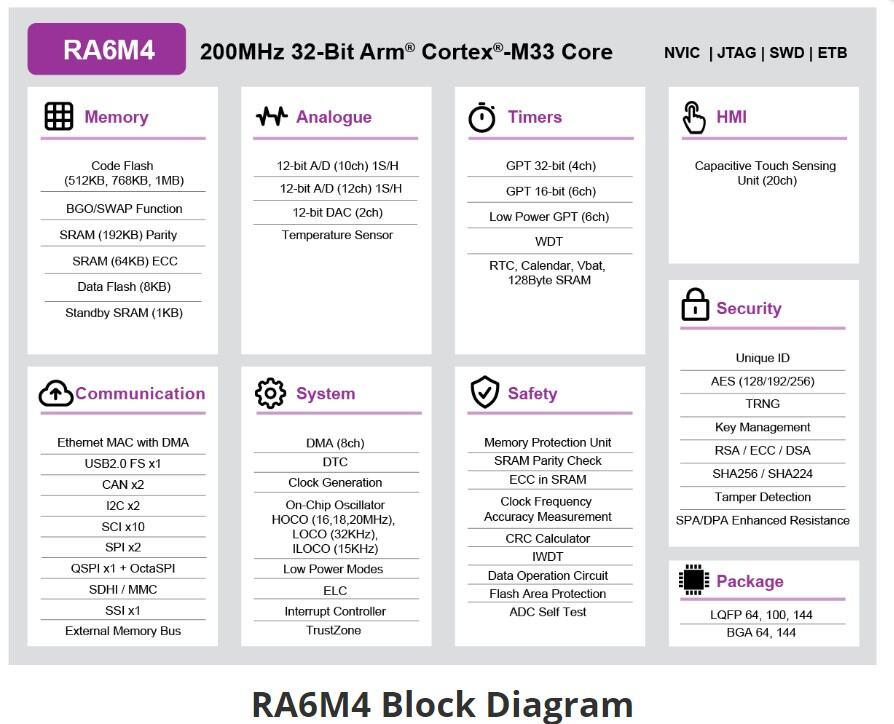
RA6M4 Block diagram (Credit: Renesas Electronics Corporation)
Detailed hardware features for the EK-RA6M4 MCU can be found at EK-RA6M4 - User’s Manual
Supported Features
The ek_ra6m4 board supports the hardware features listed below.
- on-chip / on-board
- Feature integrated in the SoC / present on the board.
- 2 / 2
-
Number of instances that are enabled / disabled.
Click on the label to see the first instance of this feature in the board/SoC DTS files. -
vnd,foo -
Compatible string for the Devicetree binding matching the feature.
Click on the link to view the binding documentation.
ek_ra6m4/r7fa6m4af3cfb target
On-target memory for this board target: 256 KiB of RAM, 1 MiB of Flash.
Type |
Location |
Description |
Compatible |
|---|---|---|---|
CPU |
on-chip |
ARM Cortex-M33 CPU1 |
|
ADC |
on-chip |
||
Clock control |
on-chip |
Renesas RA Clock Generation Circuit external clock configuration1 |
|
on-chip |
Generic fixed-rate clock provider3 |
||
on-chip |
Renesas RA Sub-Clock1 |
||
on-chip |
Renesas RA Clock Generation Circuit PLL Clock2 |
||
on-chip |
Renesas RA Clock Control node pclk block1 |
||
on-chip |
|||
on-chip |
Renesas RA External Bus Clock1 |
||
Counter |
on-chip |
Renesas RA AGT as Counter6 |
|
CRC |
on-chip |
Renesas RA CRC device1 |
|
DAC |
on-chip |
Renesas RA DAC Controller Global1 |
|
on-chip |
|||
DMA |
on-chip |
Renesas RA DMA Controller1 |
|
Ethernet |
on-chip |
Renesas RA Ethernet1 |
|
on-chip |
Renesas RA External MDIO controller1 |
||
on-board |
Generic MII PHY1 |
||
Flash controller |
on-chip |
Renesas RA family flash high-performance controller1 |
|
GPIO & Headers |
on-chip |
||
on-board |
GPIO pins exposed on Mikro BUS headers1 |
||
on-board |
GPIO pins exposed on Arduino Uno (R3) headers1 |
||
on-board |
GPIO pins exposed on a Digilent Pmod interface2 |
||
I2C |
on-chip |
||
on-chip |
Renesas RA SCI I2C controller8 |
||
Input |
on-chip |
Renesas RA Capacitive Sensing Unit1 |
|
on-board |
Group of GPIO-bound input keys1 |
||
Interrupt controller |
on-chip |
ARMv8-M NVIC (Nested Vectored Interrupt Controller)1 |
|
LED |
on-board |
Group of GPIO-controlled LEDs1 |
|
on-board |
Group of PWM-controlled LEDs1 |
||
Miscellaneous |
on-chip |
Renesas RA Event Link Controller1 |
|
on-chip |
|||
on-chip |
Renesas RA AGT6 |
||
on-chip |
|||
MMU / MPU |
on-chip |
ARMv8-M MPU (Memory Protection Unit)1 |
|
MTD |
on-chip |
Flash memory binding for Renesas RA Code flash region1 |
|
on-chip |
Flash memory binding for Renesas RA Data flash region1 |
||
on-board |
Fixed partitions of a flash (or other non-volatile storage) memory1 |
||
on-board |
Renesas RA QSPI FLASH1 |
||
PHY |
on-chip |
This binding is to be used by all the usb transceivers which are built-in with USB IP1 |
|
Pin control |
on-chip |
Renesas RA Pin Controller1 |
|
PWM |
on-chip |
||
QSPI |
on-chip |
Renesas RA QSPI1 |
|
RNG |
on-chip |
Renesas RA SCE9 TRNG1 |
|
Serial controller |
on-chip |
||
SPI |
on-chip |
Renesas RA SCI SPI controller10 |
|
on-chip |
|||
SRAM |
on-chip |
Generic on-chip SRAM1 |
|
Timer |
on-chip |
ARMv8-M System Tick1 |
|
USB |
on-chip |
Renesas RA USB full-speed controller1 |
|
on-chip |
Renesas RA USB device controller1 |
||
Watchdog |
on-chip |
Renesas RA Watchdog (wdt)1 |
Programming and Debugging
The ek_ra6m4 board supports the runners and associated west commands listed below.
| flash | debug | attach | rtt | debugserver | reset | |
|---|---|---|---|---|---|---|
| jlink | ✅ (default) | ✅ (default) | ✅ | ✅ | ✅ | ✅ |
| pyocd | ✅ | ✅ | ✅ | ✅ | ✅ | |
| rfp | ✅ |
Applications for the ek_ra6m4 board target configuration can be
built, flashed, and debugged in the usual way. See
Building an Application and Run an Application for more details on
building and running.
Note
In applications using ethernet, ethernet buffers must be placed in non-secure RAM. This requires configuration of the Implementation Defined Attribution Unit (IDAU), which must be applied by partition memory using Renesas Flash Programmer.
Partition Memory
Renesas Flash Programmer is available at (Renesas Flash Programmer Download). Once downloaded and installed, check rfp-cli is available or set rfp-cli path manually.
Renesas partition data file will be available at build/zephyr/zephyr.rpd. Connect jumper J6 then run Renesas Flash Programmer.
To partition memory manually, execute:
# From the root of the zephyr repository
rfp-cli -device ra -tool jlink -fo boundary-file build/zephyr/zephyr.rpd -p
Flashing
Program can be flashed to EK-RA6M4 via the on-board SEGGER J-Link debugger. SEGGER J-link’s drivers are available at https://www.segger.com/downloads/jlink/
To flash the program to board
Connect to J-Link OB via USB port to host PC
Make sure J-Link OB jumper is in default configuration as describe in EK-RA6M4 - User’s Manual
Execute west command to flash using jlink runner
west flash -r jlinkOr flash using rfp runner, this will partition memory then flash zephyr image.
west flash -r rfp
Debugging
You can use Segger Ozone (Segger Ozone Download) for a visual debug interface
Once downloaded and installed, open Segger Ozone and configure the debug project like so:
Target Device: R7FA6M4AF
Target Interface: SWD
Target Interface Speed: 4 MHz
Host Interface: USB
Program File: <path/to/your/build/zephyr.elf>
Note: It’s verified that we can debug OK on Segger Ozone v3.30d so please use this or later version of Segger Ozone