RA6E2 Evaluation Kit
Overview
The EK-RA6E2, an Evaluation Kit for RA6E2 MCU Group, enables users to seamlessly evaluate the features of the RA6E2 MCU group and develop embedded systems applications using Flexible Software Package (FSP) and e2 studio IDE. The users can use rich on-board features along with their choice of popular ecosystems add-ons to bring their big ideas to life
The key features of the EK-RA6E2 board are categorized in three groups as follow:
MCU Native Pin Access
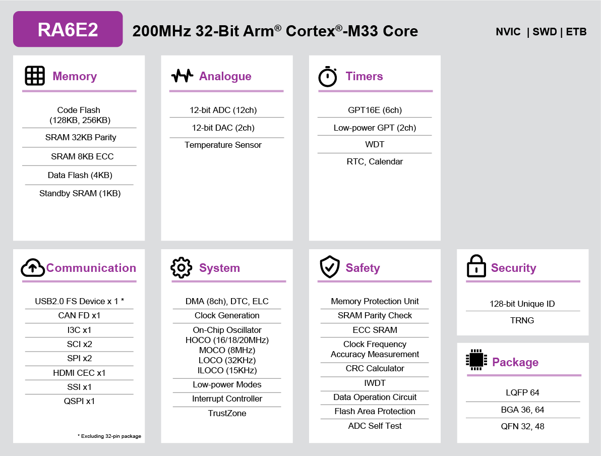
200MHz Arm Cortex-M33 based RA6E2 MCU in 64 pins, LQFP package
256 kB Code Flash, 40 kB SRAM
Native pin access through 2 x 14-pin and 1 x 40-pin male headers
MCU current measurement points for precision current consumption measurement
Multiple clock sources - RA6E2 MCU oscillator and sub-clock oscillator crystals, providing precision 20.000 MHz and 32,768 Hz reference clock. Additional low precision clocks are available internal to the RA6E2 MCU
System Control and Ecosystem Access
USB Full Speed Host and Device (micro-AB connector)
Three 5V input sources
USB (Debug, Full Speed)
External power supply (using surface mount clamp test points and J31 through holes)
Three Debug modes
Debug on-board (SWD)
Debug in (SWD)
Debug out (JTAG, SWD)
User LEDs and buttons
Three User LEDs (red, blue, green)
Power LED (white) indicating availability of regulated power
Debug LED (yellow) indicating the debug connection
Two User buttons
One Reset button
Five most popular ecosystems expansions
Two Seeed Grove system (I3C/Analog) connectors
One SparkFun Qwiic connector
Two Digilent Pmod (SPI and UART) connectors
Arduino (Uno R3) connector
MikroElektronika mikroBUS connector
MCU boot configuration jumper
Special Feature Access
16 Mb (128 Mb) External Quad-SPI Flash
CAN (3-pin header)
Hardware
Detailed hardware features for the RA6E2 MCU group can be found at RA6E2 Group User’s Manual Hardware
RA6E2 Block diagram (Credit: Renesas Electronics Corporation)
Detailed hardware features for the EK-RA6E2 MCU can be found at EK-RA6E2 - User’s Manual
Supported Features
The ek_ra6e2 board supports the hardware features listed below.
- on-chip / on-board
- Feature integrated in the SoC / present on the board.
- 2 / 2
-
Number of instances that are enabled / disabled.
Click on the label to see the first instance of this feature in the board/SoC DTS files. -
vnd,foo -
Compatible string for the Devicetree binding matching the feature.
Click on the link to view the binding documentation.
ek_ra6e2/r7fa6e2bb3cfm target
On-target memory for this board target: 40 KiB of RAM, 256 KiB of Flash.
Type |
Location |
Description |
Compatible |
|---|---|---|---|
CPU |
on-chip |
ARM Cortex-M33 CPU1 |
|
ADC |
on-chip |
Renesas RA 12-bit resolution ADC (ADC12)1 |
|
CAN |
on-chip |
Renesas RA CANFD controller global1 |
|
on-chip |
Renesas RA CANFD controller1 |
||
Clock control |
on-chip |
Renesas RA Clock Generation Circuit external clock configuration1 |
|
on-chip |
Generic fixed-rate clock provider3 |
||
on-chip |
Renesas RA Sub-Clock1 |
||
on-chip |
Renesas RA Clock Generation Circuit PLL Clock1 |
||
on-chip |
Renesas RA Clock Control node pclk block1 |
||
on-chip |
|||
Counter |
on-chip |
Renesas RA AGT as Counter2 |
|
CRC |
on-chip |
Renesas RA CRC device1 |
|
DAC |
on-chip |
Renesas RA DAC Controller Global1 |
|
on-chip |
|||
DMA |
on-chip |
Renesas RA DMA Controller1 |
|
Flash controller |
on-chip |
Renesas RA family flash high-performance controller1 |
|
GPIO & Headers |
on-chip |
||
I2C |
on-chip |
Renesas RA I2C controller2 |
|
Input |
on-chip |
Renesas RA Capacitive Sensing Unit1 |
|
on-board |
Group of GPIO-bound input keys1 |
||
Interrupt controller |
on-chip |
ARMv8-M NVIC (Nested Vectored Interrupt Controller)1 |
|
LED |
on-board |
Group of GPIO-controlled LEDs1 |
|
Miscellaneous |
on-chip |
Renesas RA Event Link Controller1 |
|
on-chip |
|||
on-chip |
|||
on-chip |
Renesas RA AGT2 |
||
MMU / MPU |
on-chip |
ARMv8-M MPU (Memory Protection Unit)1 |
|
MTD |
on-chip |
Flash memory binding for Renesas RA Code flash region1 |
|
on-chip |
Flash memory binding for Renesas RA Data flash region1 |
||
on-board |
Fixed partitions of a flash (or other non-volatile storage) memory1 |
||
on-board |
Renesas RA QSPI FLASH1 |
||
Pin control |
on-chip |
Renesas RA Pin Controller1 |
|
PWM |
on-chip |
||
QSPI |
on-chip |
Renesas RA QSPI1 |
|
RNG |
on-chip |
Renesas RA TRNG1 |
|
Serial controller |
on-chip |
||
SPI |
on-chip |
Renesas RA SCI SPI controller2 |
|
on-chip |
|||
SRAM |
on-chip |
Generic on-chip SRAM1 |
|
Timer |
on-chip |
ARMv8-M System Tick1 |
|
Watchdog |
on-chip |
Renesas RA Watchdog (wdt)1 |
Programming and Debugging
The ek_ra6e2 board supports the runners and associated west commands listed below.
| flash | debug | attach | rtt | debugserver | reset | |
|---|---|---|---|---|---|---|
| jlink | ✅ (default) | ✅ (default) | ✅ | ✅ | ✅ | ✅ |
| pyocd | ✅ | ✅ | ✅ | ✅ | ✅ |
Applications for the ek_ra6e2 board target configuration can be
built, flashed, and debugged in the usual way. See
Building an Application and Run an Application for more details on
building and running.
Flashing
Program can be flashed to EK-RA6E2 via the on-board SEGGER J-Link debugger. SEGGER J-link’s drivers are available at https://www.segger.com/downloads/jlink/
To flash the program to board
Connect to J-Link OB via USB port to host PC
Make sure J-Link OB jumper is in default configuration as describe in EK-RA6E2 - User’s Manual
Execute west command
west flash -r jlink
Debugging
You can use Segger Ozone (Segger Ozone Download) for a visual debug interface
Once downloaded and installed, open Segger Ozone and configure the debug project like so:
Target Device: R7FA6E2BB
Target Interface: SWD
Target Interface Speed: 4 MHz
Host Interface: USB
Program File: <path/to/your/build/zephyr.elf>
Note: It’s verified that we can debug OK on Segger Ozone v3.30d so please use this or later version of Segger Ozone