RA6M1 Evaluation Kit
Overview
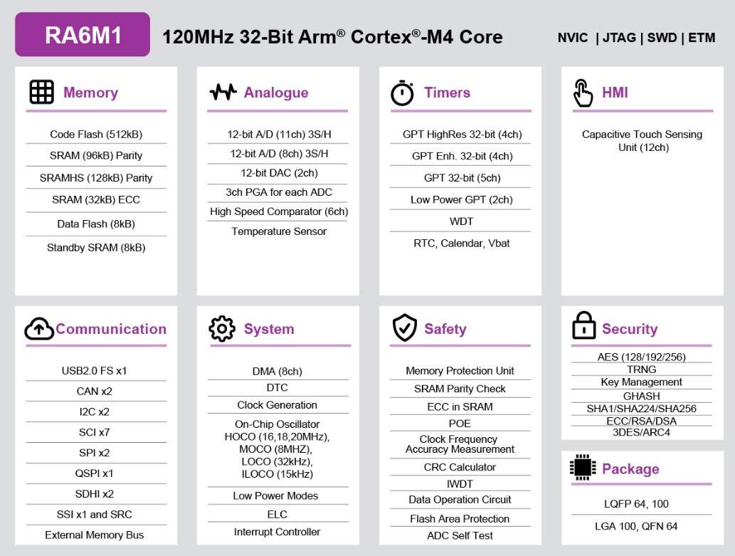
The Renesas RA6M1 microcontroller is the entry point to the Renesas RA6 product series for applications that require a high-performance Arm® Cortex®-M4 core at a very attractive price point. The RA6M1 is built on a highly efficient 40nm process and is supported by an open and flexible ecosystem concept—the Flexible Software Package (FSP), built on FreeRTOS—and is expandable to use other RTOSes and middleware. The RA6M1 is suitable for IoT applications requiring security, large embedded RAM and low power consumption.
The key features of the EK-RA6M1 board are categorized in three groups as follow:
MCU Native Pin Access
R7FA6M1AD3CFP
100-pin LQFP package
120 MHz Arm® Cortex®-M4 core with Floating Point Unit (FPU)
256 KB SRAM
512 KB code flash memory
8 KB data flash memory
Connectivity
A Device USB connector for the Main MCU
S124 MCU-based SEGGER J-Link® On-Board interface for debugging and programming of the RA6M1 MCU. A 10-pin JTAG/SWD interface is also provided for connecting optional external debuggers and programmers.
Two PMOD connectors, allowing use of appropriate PMOD compliant peripheral plug-in modules for rapid prototyping.
Pin headers for access to power and signals for the Main MCU
Multiple clock sources
Main MCU oscillator crystals, providing precision 12.000 MHz and 32,768 Hz external reference clocks
Additional low-precision clocks are available internal to the Main MCU
General purpose I/O ports
One jumper to allow measuring of Main MCU current
Copper jumpers on PCB bottom side for configuration and access to selected MCU signals
Operating voltage
External 5 V input through the Debug USB connector supplies the on-board power regulator to power logic and interfaces on the board. External 5 V or 3.3 V may be also supplied through alternate locations on the board.
A two-color board status LED indicating availability of regulated power and connection status of the J-Link interface.
A red User LED, controlled by the Main MCU firmware
A User Push-Button switch, User Capacitive Touch Button sensor, and an optional User Potentiometer, all of which are controlled by the Main MCU firmware
MCU reset push-button switch
MCU boot configuration jumper
Hardware
Detailed hardware features for the RA6M1 MCU group can be found at RA6M1 Group User’s Manual Hardware
RA6M1 Block diagram (Credit: Renesas Electronics Corporation)
Detailed hardware features for the EK-RA6M1 MCU can be found at EK-RA6M1 - User’s Manual
Supported Features
The ek_ra6m1 board supports the hardware features listed below.
- on-chip / on-board
- Feature integrated in the SoC / present on the board.
- 2 / 2
-
Number of instances that are enabled / disabled.
Click on the label to see the first instance of this feature in the board/SoC DTS files. -
vnd,foo -
Compatible string for the Devicetree binding matching the feature.
Click on the link to view the binding documentation.
ek_ra6m1/r7fa6m1ad3cfp target
On-target memory for this board target: 256 KiB of RAM, 512 KiB of Flash.
Type |
Location |
Description |
Compatible |
|---|---|---|---|
CPU |
on-chip |
ARM Cortex-M4 CPU1 |
|
ADC |
on-chip |
||
Clock control |
on-chip |
Renesas RA Clock Generation Circuit external clock configuration1 |
|
on-chip |
Generic fixed-rate clock provider3 |
||
on-chip |
Renesas RA Sub-Clock1 |
||
on-chip |
Renesas RA Clock Generation Circuit PLL Clock1 |
||
on-chip |
Renesas RA Clock Control node pclk block1 |
||
on-chip |
|||
on-chip |
Renesas RA External Bus Clock1 |
||
Counter |
on-chip |
Renesas RA AGT as Counter2 |
|
CRC |
on-chip |
Renesas RA CRC device1 |
|
DAC |
on-chip |
Renesas RA DAC Controller Global1 |
|
on-chip |
|||
DMA |
on-chip |
Renesas RA DMA Controller1 |
|
Flash controller |
on-chip |
Renesas RA family flash high-performance controller1 |
|
GPIO & Headers |
on-chip |
||
I2C |
on-chip |
Renesas RA SCI I2C controller7 |
|
on-chip |
|||
Input |
on-chip |
Renesas RA Capacitive Sensing Unit1 |
|
on-board |
Group of GPIO-bound input keys1 |
||
Interrupt controller |
on-chip |
ARMv7-M NVIC (Nested Vectored Interrupt Controller)1 |
|
LED |
on-board |
Group of GPIO-controlled LEDs1 |
|
Miscellaneous |
on-chip |
Renesas RA Event Link Controller1 |
|
on-chip |
|||
on-chip |
Renesas RA AGT2 |
||
on-chip |
|||
MMU / MPU |
on-chip |
ARMv7-M Memory Protection Unit (MPU)1 |
|
MTD |
on-chip |
Flash memory binding for Renesas RA Code flash region1 |
|
on-chip |
Flash memory binding for Renesas RA Data flash region1 |
||
on-board |
Fixed partitions of a flash (or other non-volatile storage) memory1 |
||
PHY |
on-chip |
This binding is to be used by all the usb transceivers which are built-in with USB IP1 |
|
Pin control |
on-chip |
Renesas RA Pin Controller1 |
|
PWM |
on-chip |
||
Reserved memory |
on-chip |
Renesas Option-Setting Memory3 |
|
RNG |
on-chip |
Renesas RA SCE7 TRNG1 |
|
Serial controller |
on-chip |
||
SPI |
on-chip |
Renesas RA SCI SPI controller7 |
|
on-chip |
|||
SRAM |
on-chip |
Generic on-chip SRAM1 |
|
Timer |
on-chip |
ARMv7-M System Tick1 |
|
USB |
on-chip |
Renesas RA USB full-speed controller1 |
|
on-chip |
Renesas RA USB device controller1 |
||
Watchdog |
on-chip |
Renesas RA Watchdog (wdt)1 |
Programming and Debugging
The ek_ra6m1 board supports the runners and associated west commands listed below.
| flash | debug | attach | rtt | debugserver | reset | |
|---|---|---|---|---|---|---|
| jlink | ✅ (default) | ✅ (default) | ✅ | ✅ | ✅ | ✅ |
| pyocd | ✅ | ✅ | ✅ | ✅ | ✅ |
Applications for the ek_ra6m1 board target configuration can be
built, flashed, and debugged in the usual way. See
Building an Application and Run an Application for more details on
building and running.
Flashing
Program can be flashed to EK-RA6M1 via the on-board SEGGER J-Link debugger. SEGGER J-link’s drivers are available at https://www.segger.com/downloads/jlink/
To flash the program to board
Connect to J-Link OB via USB port to host PC
Make sure J-Link OB jumper is in default configuration as describe in EK-RA6M1 - User’s Manual
Execute west command
west flash -r jlink
Debugging
You can use Segger Ozone (Segger Ozone Download) for a visual debug interface
Once downloaded and installed, open Segger Ozone and configure the debug project like so:
Target Device: R7FA6M1AD
Target Interface: SWD
Target Interface Speed: 4 MHz
Host Interface: USB
Program File: <path/to/your/build/zephyr.elf>
Note: It’s verified that we can debug OK on Segger Ozone v3.30d so please use this or later version of Segger Ozone