Nucleo F412ZG
Overview
The Nucleo F412ZG board features an ARM Cortex-M4 based STM32F412ZG MCU with a wide range of connectivity support and configurations. Here are some highlights of the Nucleo F412ZG board:
STM32 microcontroller in LQFP144 package
Two types of extension resources:
ST Zio connector including: support for Arduino* Uno V3 connectivity (A0 to A5, D0 to D15) and additional signals exposing a wide range of peripherals
ST morpho extension pin headers for full access to all STM32 I/Os
On-board ST-LINK/V2-1 debugger/programmer with SWD connector
Flexible board power supply:
5 V from ST-LINK/V2-1 USB VBUS
External power sources: 3.3 V and 7 - 12 V on ST Zio or ST morpho connectors, 5 V on ST morpho connector
Three user LEDs
Two push-buttons: USER and RESET
More information about the board can be found at the Nucleo F412ZG website.
Hardware
Nucleo F412ZG provides the following hardware components:
STM32F412ZGT6 in LQFP144 package
ARM® 32-bit Cortex®-M4 CPU with FPU
100 MHz max CPU frequency
VDD from 1.7 V to 3.6 V
1 MB Flash
256 KB SRAM
GPIO with external interrupt capability
12-bit ADC with 16 channels, with FIFO and burst support
RTC
14 General purpose timers
2 watchdog timers (independent and window)
SysTick timer
USART/UART (4)
I2C (4)
SPI (5)
SDIO
USB 2.0 OTG FS
DMA Controller
CRC calculation unit
More information about STM32F412ZG can be found here:
Supported Features
The nucleo_f412zg board supports the hardware features listed below.
- on-chip / on-board
- Feature integrated in the SoC / present on the board.
- 2 / 2
-
Number of instances that are enabled / disabled.
Click on the label to see the first instance of this feature in the board/SoC DTS files. -
vnd,foo -
Compatible string for the Devicetree binding matching the feature.
Click on the link to view the binding documentation.
nucleo_f412zg/stm32f412zx target
On-target memory for this board target: 256 KiB of RAM, 1 MiB of Flash.
Type |
Location |
Description |
Compatible |
|---|---|---|---|
CPU |
on-chip |
ARM Cortex-M4F CPU1 |
|
ADC |
on-chip |
STM32F4 ADC1 |
|
CAN |
on-chip |
STM32 CAN controller2 |
|
Clock control |
on-chip |
STM32F4 RCC (Reset and Clock controller)1 |
|
on-chip |
STM32 HSE Clock1 |
||
on-chip |
|||
on-chip |
|||
on-chip |
STM32 Clock multiplexer1 |
||
on-chip |
STM32 Microcontroller Clock Output (MCO)2 |
||
Counter |
on-chip |
STM32 counters14 |
|
DMA |
on-chip |
STM32 DMA controller (V1)2 |
|
Flash controller |
on-chip |
STM32 Family flash controller1 |
|
GPIO & Headers |
on-chip |
STM32 GPIO Controller8 |
|
on-board |
GPIO pins exposed on Arduino Uno (R3) headers1 |
||
I2C |
on-chip |
||
I2S |
on-chip |
STM32 I2S controller4 |
|
Input |
on-board |
Group of GPIO-bound input keys1 |
|
Interrupt controller |
on-chip |
ARMv7-M NVIC (Nested Vectored Interrupt Controller)1 |
|
on-chip |
STM32 External Interrupt Controller1 |
||
LED |
on-board |
Group of GPIO-controlled LEDs1 |
|
Memory controller |
on-chip |
STM32 Battery Backed RAM1 |
|
MMC |
on-chip |
STM32 SDMMC Host Controller1 |
|
MTD |
on-chip |
STM32F4 flash memory1 |
|
NVMEM |
on-chip |
Fixed layout for Non-Volatile memory1 |
|
OTP memory |
on-chip |
||
PHY |
on-chip |
This binding is to be used by all the usb transceivers which are built-in with USB IP1 |
|
Pin control |
on-chip |
STM32 Pin controller1 |
|
Power management |
on-chip |
STM32 power controller1 |
|
PWM |
on-chip |
||
QSPI |
on-chip |
STM32 QSPI Controller1 |
|
Reset controller |
on-chip |
STM32 Reset and Clock Control (RCC) Controller1 |
|
RNG |
on-chip |
STM32 Random Number Generator1 |
|
RTC |
on-chip |
STM32 RTC1 |
|
Sensors |
on-chip |
STM32 quadrature decoder6 |
|
on-chip |
STM32 family TEMP node for production calibrated sensors with two calibration temperatures1 |
||
on-chip |
STM32 VREF+1 |
||
on-chip |
STM32 VBAT1 |
||
Serial controller |
on-chip |
||
SMbus |
on-chip |
STM32 SMBus controller3 |
|
SPI |
on-chip |
||
Timer |
on-chip |
ARMv7-M System Tick1 |
|
on-chip |
|||
USB |
on-chip |
STM32 OTGFS controller1 |
|
Watchdog |
on-chip |
STM32 watchdog1 |
|
on-chip |
STM32 system window watchdog1 |
Connections and IOs
Nucleo F412ZG Board has 8 GPIO controllers. These controllers are responsible for pin muxing, input/output, pull-up, etc.
Available pins:
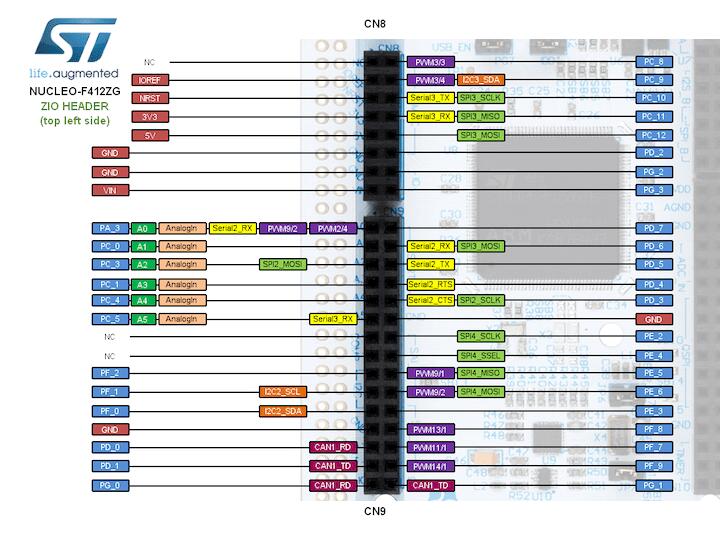
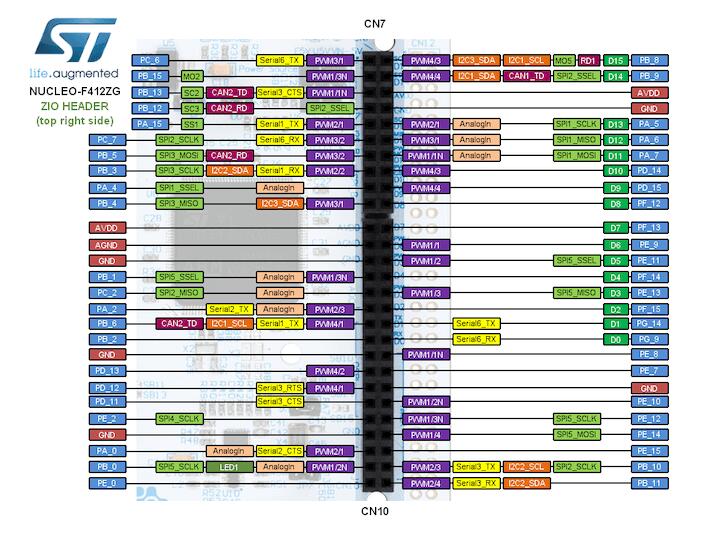
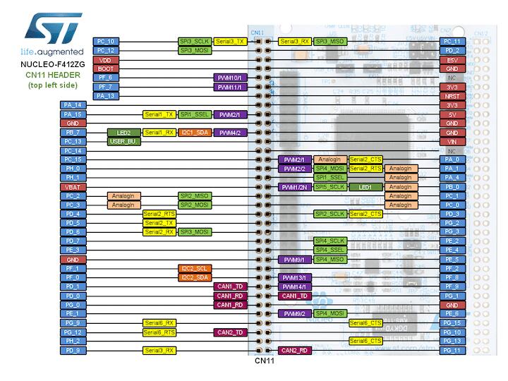
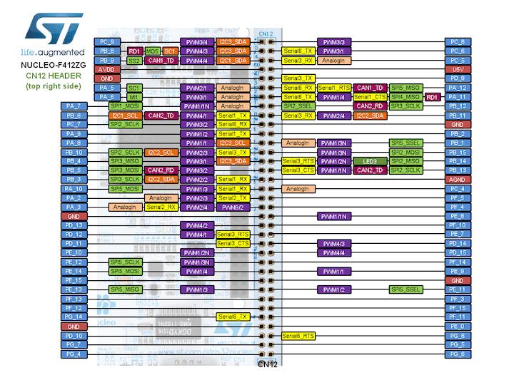
For more details please refer to STM32 Nucleo-144 board User Manual.
Default Zephyr Peripheral Mapping:
UART_3 TX/RX : PD8/PD9 (ST-Link Virtual Port Com)
UART_6 TX/RX : PG14/PG9 (Arduino Serial)
I2C1 SCL/SDA : PB8/PB9 (Arduino I2C)
SPI1 NSS/SCK/MISO/MOSI : PD14/PA5/PA6/PA7 (Arduino SPI)
PWM_2_CH1 : PA0
USER_PB : PC13
LD1 : PB0
LD2 : PB7
LD3 : PB14
USB DM : PA11
USB DP : PA12
System Clock
Nucleo F412ZG System Clock could be driven by internal or external oscillator, as well as main PLL clock. By default System clock is driven by PLL clock at 96MHz, driven by 8MHz high speed external clock.
Serial Port
Nucleo F412ZG board has 4 UARTs. The Zephyr console output is assigned to UART3. Default settings are 115200 8N1.
Network interface
Ethernet over USB is configured as the default network interface
Programming and Debugging
The nucleo_f412zg board supports the runners and associated west commands listed below.
| flash | debug | attach | rtt | debugserver | reset | |
|---|---|---|---|---|---|---|
| jlink | ✅ | ✅ | ✅ | ✅ | ✅ | ✅ |
| openocd | ✅ | ✅ (default) | ✅ | ✅ | ✅ | |
| stm32cubeprogrammer | ✅ (default) |
Nucleo F412ZG board includes an ST-LINK/V2-1 embedded debug tool interface.
Flashing
The board is configured to be flashed using west STM32CubeProgrammer runner, so its installation is required.
Alternatively, OpenOCD or JLink can also be used to flash the board using
the --runner (or -r) option:
$ west flash --runner openocd
$ west flash --runner jlink